SNVS188I May 2004 – October 2017 LM2623
PRODUCTION DATA.
- 1 Features
- 2 Applications
- 3 Description
- 4 Revision History
- 5 Pin Configuration And Functions
- 6 Specifications
- 7 Detailed Description
- 8 Applications And Implementation
- 9 Power Supply Recommendations
- 10Layout
- 11Device And Documentation Support
- 12Mechanical, Packaging, And Orderable Information
1 Features
- Good Efficiency Over a Very Wide Load Range
- Very Low Output Voltage Ripple
- Up to 2-MHz Switching Frequency
- 0.8-V to 14-V Operating Voltage
- 1.1-V Start-up Voltage
- 1.24-V to 14-V Adjustable Output Voltage
- Up to 2-A Load Current at Low Output Voltages
- 0.17-Ω Internal MOSFET
- Up to 90% Regulator Efficiency
- 80-µA Typical Operating Current (Into VDD Pin of Supply)
- < 2.5-µA Ensured Supply Current In Shutdown
- Small 8-Pin VSSOP Package (Half the Footprint of Standard 8-Pin SOIC Package); 1.09-mm Package Height
- 4-mm × 4-mm Thermally Enhanced WSON Package Option
2 Applications
- Cameras, Pagers and Cell Phones
- PDAs, Palmtop Computers, GPS devices
- White LED Drive, TFT, or Scanned LCDs
- Flash Memory Programming
- Hand-Held Instruments
- 1, 2, 3, or 4 Cell Alkaline Systems
- 1, 2, or 3 Cell Lithium-ion Systems
3 Description
The LM2623 is a high-efficiency, general-purpose, step-up DC-DC switching regulator for battery-powered and low input voltage systems. It accepts an input voltage between 0.8 V and 14 V and converts it into a regulated output voltage between 1.24 V and 14 V. Efficiencies up to 90% are achievable with the LM2623.
In order to adapt to a number of applications, the LM2623 allows the designer to vary the output voltage, the operating frequency (300 kHz to 2 MHz) and duty cycle (17% to 90%) to optimize the part's performance. The selected values can be fixed or can vary with battery voltage or input to output voltage ratio. The LM2623 uses a very simple, on/off regulation mode to produce good efficiency and stable operation over a wide operating range. It normally regulates by skipping switching cycles when it reaches the regulation limit (Pulse Frequency Modulation).
Note: See Non-Linear Effect and Choosing The Correct C3 Capacitor so that any challenges with designing with this part can be taken into account before a board design/layout is finalized.
For alternative solutions, See Also: LM2700, LM2622, LM2731, LM2733, and LM2621.
Device Information(1)
| PART NUMBER | PACKAGE | BODY SIZE (NOM) |
|---|---|---|
| LM2623 | WSON (14) | 4.00 mm × 4.00 mm |
| VSSOP (8) | 3.00 mm × 3.00 mm |
- For all available packages, see the orderable addendum at the end of the data sheet.
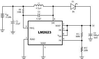
Typical Application Circuit
