ZHCSNR6G June 1999 – March 2023 LM2576 , LM2576HV
PRODUCTION DATA
- 1 特性
- 2 应用
- 3 说明
- 4 Revision History
- 5 Pin Configuration and Functions
-
6 Specifications
- 6.1 Absolute Maximum Ratings
- 6.2 ESD Ratings
- 6.3 Recommended Operating Conditions
- 6.4 Thermal Information
- 6.5 Electrical Characteristics: 3.3 V
- 6.6 Electrical Characteristics: 5 V
- 6.7 Electrical Characteristics: 12 V
- 6.8 Electrical Characteristics: 15 V
- 6.9 Electrical Characteristics: Adjustable Output Voltage
- 6.10 Electrical Characteristics: All Output Voltage Versions
- 6.11 Typical Characteristics
- 7 Detailed Description
- 8 Application and Implementation
- 9 Device and Documentation Support
- 10Mechanical, Packaging, and Orderable Information
封装选项
请参考 PDF 数据表获取器件具体的封装图。
机械数据 (封装 | 引脚)
- NDH|5
- NEB|5
- KTT|5
- KC|5
散热焊盘机械数据 (封装 | 引脚)
- KTT|5
订购信息
5 Pin Configuration and Functions
 Figure 5-1 KC Package
5-Pin TO-220Top
View
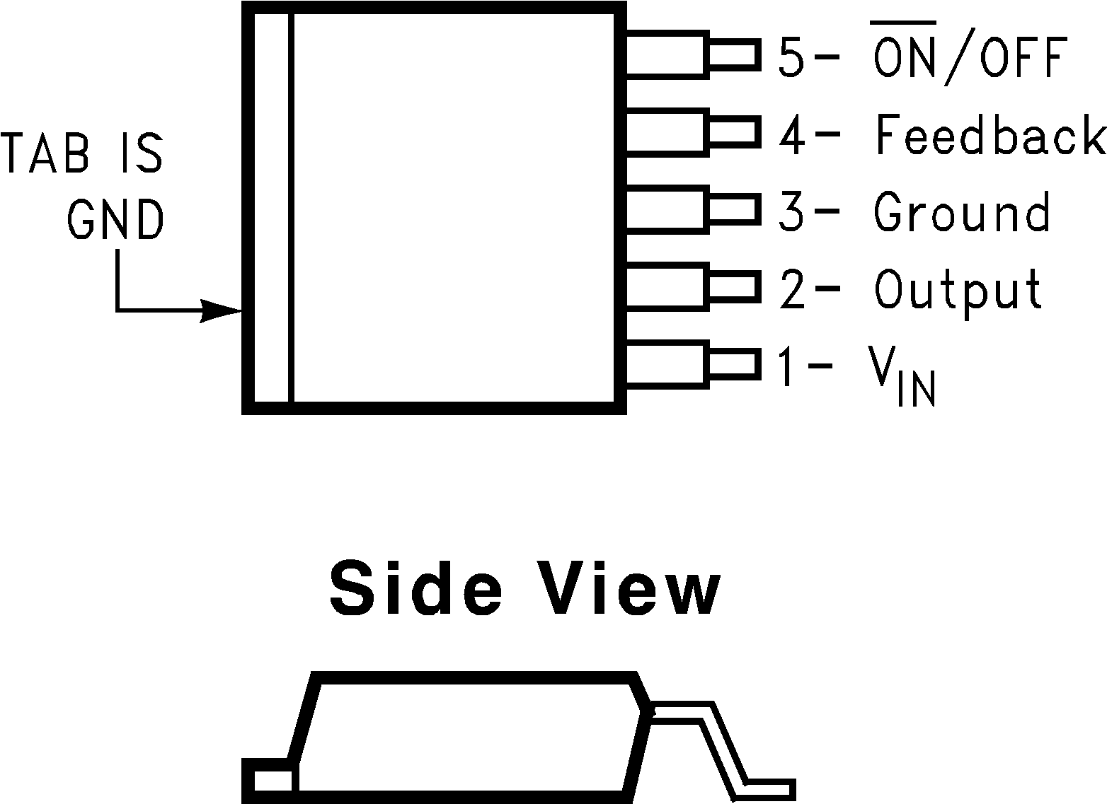
 Figure 5-2 KTT Package5-PIN DDPAK/TO-263Top
View
 Figure 5-3 DDPAK/TO-263 (S) Package5-Lead Surface-Mount PackageTop View
Table 5-1 Pin Functions
| PIN | I/O(1) | DESCRIPTION | |
|---|---|---|---|
| NO. | NAME | ||
| 1 | VIN | I | Supply input pin to collector pin of high-side transistor. Connect to power supply and input bypass capacitors CIN. Path from VIN pin to high frequency bypass CIN and GND must be as short as possible. |
| 2 | OUTPUT | O | Emitter pin of the power transistor. This is a switching node. Attached this pin to an inductor and the cathode of the external diode. |
| 3 | GROUND | — | Ground pin. Path to CIN must be as short as possible. |
| 4 | FEEDBACK | I | Feedback sense input pin. Connect to the midpoint of feedback divider to set VOUT for ADJ version or connect this pin directly to the output capacitor for a fixed output version. |
| 5 | ON/OFF | I | Enable input to the voltage regulator. High = OFF and low = ON. Connect to GND to enable the voltage regulator. Do not leave this pin float. |
| — | TAB | — | Connected to GND. Attached to heatsink for thermal relief for TO-220 package or put a copper plane connected to this pin as a thermal relief for DDPAK package. |
(1) I = INPUT, O = OUTPUT