SLVS047L November 1981 – January 2015 LM237 , LM337
PRODUCTION DATA.
- 1 Features
- 2 Applications
- 3 Description
- 4 Simplified Schematic
- 5 Revision History
- 6 Pin Configuration and Functions
- 7 Specifications
- 8 Detailed Description
- 9 Application and Implementation
- 10Power Supply Recommendations
- 11Layout
- 12Device and Documentation Support
- 13Mechanical, Packaging, and Orderable Information
7 Specifications
7.1 Absolute Maximum Ratings
over operating temperature ranges (unless otherwise noted)(1)| MIN | MAX | UNIT | |||
|---|---|---|---|---|---|
| VI – VO | Input-to-output differential voltage | –40 | V | ||
| TJ | Operating virtual junction temperature | 150 | °C | ||
| Lead temperature | 1.6 mm (1/16 in) from case for 10 s | 260 | °C | ||
| Tstg | Storage temperature range | –65 | 150 | °C | |
(1) Stresses beyond those listed under Absolute Maximum Ratings may cause permanent damage to the device. These are stress ratings only, and functional operation of the device at these or any other conditions beyond those indicated under Recommended Operating Conditions is not implied. Exposure to absolute-maximum-rated conditions for extended periods may affect device reliability.
7.2 ESD Ratings
| VALUE | UNIT | |||
|---|---|---|---|---|
| V(ESD) | Electrostatic discharge | Human body model (HBM), per ANSI/ESDA/JEDEC JS-001, all pins(1) | 1500 | V |
| Charged device model (CDM), per JEDEC specification JESD22-C101, all pins(2) | 1500 | |||
(1) JEDEC document JEP155 states that 500-V HBM allows safe manufacturing with a standard ESD control process.
(2) JEDEC document JEP157 states that 250-V CDM allows safe manufacturing with a standard ESD control process.
7.3 Recommended Operating Conditions
| MIN | MAX | UNIT | |||
|---|---|---|---|---|---|
| VI-VO | Input-to-output differential voltage | -2.5 | -37 | ||
| IO | Output current | |VI – VO| ≤ 40 V, P ≤ 15 W | 10 | 1500 | mA |
| |VI – VO| ≤ 10 V, P ≤ 15 W | 6 | 1500 | |||
| TJ | Operating virtual junction temperature | LM237 | –25 | 150 | °C |
| LM337 | 0 | 125 |
7.4 Thermal Information
| THERMAL METRIC(1) | LM237 | LMx37 | LM337 | UNIT | ||||
|---|---|---|---|---|---|---|---|---|
| KC | KCS | KTE | KTP | KTT | KVU | |||
| 4 PINS | 4 PINS | 4 PINS | 4 PINS | 4 PINS | 4 PINS | |||
| RθJA | Junction-to-ambient thermal resistance | 24.8 | 24.8 | 23 | 28 | 25.3 | 30.3 | °C/W |
| RθJC(top) | Junction-to-case (top) thermal resistance | 3 | 3 | 3 | 19 | 30.3 | N/A | |
(1) For more information about traditional and new thermal metrics, see the IC Package Thermal Metrics application report (SPRA953).
7.5 Electrical Characteristics
over recommended ranges of operating virtual junction temperature (unless otherwise noted)| PARAMETER | TEST CONDITIONS(1) | LM237 | LM337 | UNIT | |||||
|---|---|---|---|---|---|---|---|---|---|
| MIN | TYP | MAX | MIN | TYP | MAX | ||||
| Input regulation(2) | VI – VO = –3 V to –40 V | TJ = 25°C | 0.01 | 0.02 | 0.01 | 0.04 | %/V | ||
| TJ = MIN to MAX | 0.02 | 0.05 | 0.02 | 0.07 | |||||
| Ripple rejection | VO = –10 V, f = 120 Hz | 60 | 60 | dB | |||||
| VO = –10 V, f = 120 Hz, CADJ = 10 μF | 66 | 77 | 66 | 77 | |||||
| Output regulation | IO = 10 mA to 1.5 A, TJ = 25°C |
|VO| ≤ 5 V | 25 | 50 | mV | ||||
| |VO| ≥ 5 V | 0.3% | 0.5% | 0.3% | 1% | — | ||||
| IO = 10 mA to 1.5 A | |VO| ≤ 5 V | 50 | 70 | mV | |||||
| |VO| ≥ 5 V | 1% | 1.5% | — | ||||||
| Output-voltage change with temperature | TJ = MIN to MAX | 0.6% | 0.6% | — | |||||
| Output-voltage long-term drift | After 1000 h at TJ = MAX and VI – VO = –40 V | 0.3% | 1% | 0.3% | 1% | — | |||
| Output noise voltage | f = 10 Hz to 10 kHz, TJ = 25°C | 0.003% | 0.003% | — | |||||
| Minimum output current to maintain regulation | |VI – VO| ≤ 40 V | 2.5 | 5 | 2.5 | 10 | mA | |||
| |VI – VO| ≤ 10 V | 1.2 | 3 | 1.5 | 6 | |||||
| Peak output current | |VI – VO| ≤ 15 V | 1.5 | 2.2 | 1.5 | 2.2 | A | |||
| |VI – VO| ≤ 40 V, TJ = 25°C | 0.24 | 0.4 | 0.15 | 0.4 | |||||
| ADJUSTMENT current | 65 | 100 | 65 | 100 | μA | ||||
| Change in ADJUSTMENT current | VI – VO = –2.5 V to –40 V, IO = 10 mA to MAX, TJ = 25°C | 2 | 5 | 2 | 5 | μA | |||
| Reference voltage (OUTPUT to ADJUSTMENT) | VI – VO = –3 V to –40 V, IO = 10 mA to 1.5 A, P ≤ rated dissipation |
TJ = 25°C | –1.225 | –1.25 | –1.275 | –1.213 | –1.25 | –1.287 | V |
| TJ = MIN to MAX | –1.2 | –1.25 | –1.3 | –1.2 | –1.25 | –1.3 | |||
| Thermal regulation | Initial TJ = 25°C, 10-ms pulse | 0.002 | 0.02 | 0.003 | 0.04 | %/W | |||
(1) Unless otherwise noted, the following test conditions apply: |VI – VO| = 5 V and IO = 0.5 A. For conditions shown as MIN or MAX, use the appropriate value specified under recommended operating conditions. All characteristics are measured with a 0.1-μF capacitor across the input and a 1-μF capacitor across the output. Pulse-testing techniques are used to maintain the junction temperature as close to the ambient temperature as possible. Thermal effects must be taken into account separately.
(2) Input regulation is expressed here as the percentage change in output voltage per 1-V change at the input.
7.6 Electrical Characteristics
TJ = 25°C| PARAMETER | TEST CONDITIONS(1) | LM237, LM337 | UNIT | |||
|---|---|---|---|---|---|---|
| MIN | TYP | MAX | ||||
| Input regulation(2) | VI – VO = –3 V to –40 V | 0.01 | 0.04 | %/V | ||
| Ripple rejection | VO = –10 V, f = 120 Hz | 60 | dB | |||
| VO = –10 V, f = 120 Hz, CADJ = 10 μF | 66 | 77 | ||||
| Output regulation | IO = 10 mA to 1.5 A | |VO| ≤ 5 V | 50 | mV | ||
| |VO| ≥ 5 V | 0.3% | 1% | — | |||
| Output noise voltage | f = 10 Hz to 10 kHz | 0.003% | — | |||
| Minimum output current to maintain regulation | |VI – VO| ≤ 40 V | 2.5 | 10 | mA | ||
| |VI – VO| ≤ 10 V | 1.5 | 6 | ||||
| Peak output current | |VI – VO| ≤ 15 V | 1.5 | 2.2 | A | ||
| |VI – VO| ≤ 40 V | 0.15 | 0.4 | ||||
| ADJUSTMENT current | 65 | 100 | μA | |||
| Change in ADJUSTMENT current | VI – VO = –2.5 V to –40 V, IO = 10 mA to MAX | 2 | 5 | μA | ||
| Reference voltage (OUTPUT to ADJUSTMENT) |
VI – VO = –3 V to –40 V, IO = 10 mA to 1.5 A, P ≤ rated dissipation | –1.213 | –1.25 | –1.287 | V | |
(1) Unless otherwise noted, the following test conditions apply: |VI – VO| = 5 V and IO = 0.5 A. All characteristics are measured with a 0.1-μF capacitor across the input and a 1-μF capacitor across the output. Pulse-testing techniques are used to maintain the junction temperature as close to the ambient temperature as possible. Thermal effects must be taken into account separately.
(2) Input regulation is expressed here as the percentage change in output voltage per 1-V change at the input.
7.7 Typical Characteristics
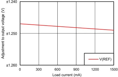 Figure 1. Adjustment Voltage vs Load current (VIN = -4.3 V)