SNIS106Q December 1999 – January 2015 LM20
PRODUCTION DATA.
- 1 Features
- 2 Applications
- 3 Description
- 4 Revision History
- 5 Pin Configuration and Functions
- 6 Specifications
- 7 Detailed Description
- 8 Application and Implementation
- 9 Power Supply Recommendations
- 10Layout
- 11Device and Documentation Support
- 12Mechanical, Packaging, and Orderable Information
6 Specifications
6.1 Absolute Maximum Ratings
over operating free-air temperature range (unless otherwise noted)(1)(3)| MIN | MAX | UNIT | ||
|---|---|---|---|---|
| Supply Voltage | −0.2 | 6.5 | V | |
| Output Voltage | −0.6 | (V+ + 0.6 ) | V | |
| Output Current | 10 | mA | ||
| Input Current at any pin(2) | 5 | mA | ||
| Maximum Junction Temperature (TJMAX) | 150 | °C | ||
| Storage temperature, Tstg | −65 | 150 | °C | |
(1) Stresses beyond those listed under Absolute Maximum Ratings may cause permanent damage to the device. These are stress ratings only, which do not imply functional operation of the device at these or any other conditions beyond those indicated under Recommended Operating Conditions. Exposure to absolute-maximum-rated conditions for extended periods may affect device reliability.
(2) When the input voltage (VI) at any pin exceeds power supplies (VI < GND or VI > V+), the current at that pin should be limited to 5 mA.
(3) Soldering process must comply with TI's Reflow Temperature Profile specifications. Refer to http://www.ti.com/packaging.
6.2 ESD Ratings
| VALUE | UNIT | |||
|---|---|---|---|---|
| V(ESD) | Electrostatic discharge | Human-body model (HBM), per ANSI/ESDA/JEDEC JS-001(1) | ±2500 | V |
| Charged-device model (CDM), per JEDEC specification JESD22-C101(2) | ±250 | |||
(1) JEDEC document JEP155 states that 500-V HBM allows safe manufacturing with a standard ESD control process.
(2) JEDEC document JEP157 states that 250-V CDM allows safe manufacturing with a standard ESD control process.
6.3 Recommended Operating Conditions
over operating free-air temperature range (unless otherwise noted)(1)| MIN | MAX | UNIT | ||
|---|---|---|---|---|
| LM20B, LM20C with 2.4 V ≤ V+≤ 2.7 V | −30 | 130 | °C | |
| LM20B, LM20C with 2.7 V ≤ V+≤ 5.5 V | −55 | 130 | °C | |
| LM20S with 2.4 V ≤ V+≤ 5.5 V | −30 | 125 | °C | |
| LM20S with 2.7 V ≤ V+≤ 5.5 V | −40 | 125 | °C | |
| Supply Voltage Range (V+) | 2.4 | 5.5 | V | |
(1) Stresses beyond those listed under Absolute Maximum Ratings may cause permanent damage to the device. These are stress ratings only, which do not imply functional operation of the device at these or any other conditions beyond those indicated under Recommended Operating Conditions. Exposure to absolute-maximum-rated conditions for extended periods may affect device reliability.
6.4 Thermal Information
| THERMAL METRIC(1) | LM20 | UNIT | ||
|---|---|---|---|---|
| DCK (SC70) | YZR (DSBGA) | |||
| 5 PINS | 4 PINS | |||
| RθJA | Junction-to-ambient thermal resistance | 282 | 197 | °C/W |
| RθJC(top) | Junction-to-case (top) thermal resistance | 93 | 2 | |
| RθJB | Junction-to-board thermal resistance | 62 | 40 | |
| ψJT | Junction-to-top characterization parameter | 1.6 | 11 | |
| ψJB | Junction-to-board characterization parameter | 62 | 40 | |
| RθJC(bot) | Junction-to-case (bottom) thermal resistance | — | — | |
(1) For more information about traditional and new thermal metrics, see the IC Package Thermal Metrics application report, SPRA953.
6.5 Electrical Characteristics: LM20B
Unless otherwise noted, these specifications apply for V+ = 2.7 VDC. All limits TA = TJ = TMIN to TMAX, unless otherwise noted.| PARAMETER | TEST CONDITIONS | MIN(1) | TYP(2) | MAX(1) | UNIT |
|---|---|---|---|---|---|
| Temperature to Voltage Error VO = (−3.88×10⁻⁶× T 2) + (−1.15×10⁻²× T) + 1.8639 V(3) |
TA = 25°C to 30°C | –1.5 | 1.5 | °C | |
| TA = 130°C | –2.5 | 2.5 | °C | ||
| TA = 125°C | –2.5 | 2.5 | °C | ||
| TA = 100°C | –2.2 | 2.2 | °C | ||
| TA = 85°C | –2.1 | 2.1 | °C | ||
| TA = 80°C | –2.0 | 2.0 | °C | ||
| TA = 0°C | –1.9 | 1.9 | °C | ||
| TA = –30°C | –2.2 | 2.2 | °C | ||
| TA = –40°C | –2.3 | 2.3 | °C | ||
| TA = –55°C | –2.5 | 2.5 | °C | ||
| Output Voltage at 0°C | 1.8639 | V | |||
| Variance from Curve | ±1.0 | °C | |||
| Non-linearity(4) | –20°C ≤ TA ≤ 80°C | ±0.4% | |||
| Sensor Gain (Temperature Sensitivity or Average Slope) to equation: VO=−11.77 mV / °C×T+1.860 V |
–30°C ≤ TA ≤ 100°C | –12.2 | –11.77 | –11.4 | mV/°C |
| Output Impedance | Sourcing IL 0 μA to 16 μA(6)(7) | 160 | Ω | ||
| Load Regulation(5) | Sourcing IL 0 μA to 16 μA(3)(7) | –2.5 | mV | ||
| Line Regulation(8) | 2.4 V ≤ V+ ≤ 5.0 V | 3.3 | mV/V | ||
| 5.0 V ≤ V+ ≤ 5.5 V | 11 | mV | |||
| Quiescent Current | 2.4 V ≤ V+ ≤ 5.0 V; TA = 25°C | 4.5 | 7 | μA | |
| 5.0 V ≤ V+ ≤ 5.5 V; TA = 25°C | 4.5 | 9 | μA | ||
| 2.4 V ≤ V+ ≤ 5.0 V | 4.5 | 10 | μA | ||
| Change of Quiescent Current | 2.4 V ≤ V+ ≤ 5.5 V | 0.7 | μA | ||
| Temperature Coefficient of Quiescent Current | –11 | nA/°C | |||
| Shutdown Current | V+ ≤ 0.8 V | 0.02 | μA |
(1) Limits are ensured to TI's AOQL (Average Outgoing Quality Level).
(2) Typicals are at TJ = TA = 25°C and represent most likely parametric norm.
(3) Accuracy is defined as the error between the measured and calculated output voltage at the specified conditions of voltage, current, and temperature (expressed in °C).
(4) Non-linearity is defined as the deviation of the calculated output-voltage-versus-temperature curve from the best-fit straight line, over the temperature range specified.
(5) Regulation is measured at constant junction temperature, using pulse testing with a low duty cycle. Changes in output due to heating effects can be computed by multiplying the internal dissipation by the thermal resistance.
(6) The LM20 can at most sink 1 μA and source 16 μA.
(7) Load regulation or output impedance specifications apply over the supply voltage range of 2.4 V to 5.5 V.
(8) Line regulation is calculated by subtracting the output voltage at the highest supply input voltage from the output voltage at the lowest supply input voltage.
6.6 Electrical Characteristics: LM20C
Unless otherwise noted, these specifications apply for V+ = 2.7 VDC. All limits TA = TJ = TMIN to TMAX, unless otherwise noted.| PARAMETER | TEST CONDITIONS | MIN(1) | TYP(2) | MAX(1) | UNIT |
|---|---|---|---|---|---|
| Temperature to Voltage Error VO = (−3.88×10⁻⁶× T 2) + (−1.15×10⁻²× T) + 1.8639 V(3) |
TA = 25°C to 30°C | –4 | 5 | °C | |
| TA = 130°C | –5 | 5 | °C | ||
| TA = 125°C | –5 | 5 | °C | ||
| TA = 100°C | –4.7 | 4.7 | °C | ||
| TA = 85°C | –4.6 | 4.6 | °C | ||
| TA = 80°C | –4.5 | 4.5 | °C | ||
| TA = 0°C | –4.4 | 4.4 | °C | ||
| TA = –30°C | –4.7 | 4.7 | °C | ||
| TA = –40°C | –4.8 | 4.8 | °C | ||
| TA = –55°C | –5.0 | 5.0 | °C | ||
| Output Voltage at 0°C | 1.8639 | V | |||
| Variance from Curve | ±1.0 | °C | |||
| Non-Linearity (4) | –20°C ≤ TA ≤ 80°C | ±0.4% | |||
| Sensor Gain (Temperature Sensitivity or Average Slope) to equation: VO=−11.77 mV / °C×T+1.860 V |
–30°C ≤ TA ≤ 100°C | –12.6 | –11.77 | –11.0 | mV/°C |
| Output Impedance | Sourcing IL 0 μA to 16 μA (6)(7) | 160 | Ω | ||
| Load Regulation(5) | Sourcing IL 0 μA to 16 μA (6)(7) | –2.5 | mV | ||
| Line Regulation(8) | 2.4 V ≤ V+ ≤ 5.0 V | 3.7 | mV/V | ||
| 5.0 V ≤ V+ ≤ 5.5 V | 11 | mV | |||
| Quiescent Current | 2.4 V ≤ V+ ≤ 5.0 V; TA = 25°C | 4.5 | 7 | μA | |
| 5.0 V ≤ V+ ≤ 5.5 V; TA = 25°C | 4.5 | 9 | μA | ||
| 2.4 V ≤ V+ ≤ 5.0 V | 4.5 | 10 | μA | ||
| Change of Quiescent Current | 2.4 V ≤ V+ ≤ 5.5 V | 0.7 | μA | ||
| Temperature Coefficient of Quiescent Current | –11 | nA/°C | |||
| Shutdown Current | V+ ≤ 0.8 V | 0.02 | μA |
(1) Limits are ensured to TI's AOQL (Average Outgoing Quality Level).
(2) Typicals are at TJ = TA = 25°C and represent most likely parametric norm.
(3) Accuracy is defined as the error between the measured and calculated output voltage at the specified conditions of voltage, current, and temperature (expressed in °C).
(4) Non-linearity is defined as the deviation of the calculated output-voltage-versus-temperature curve from the best-fit straight line, over the temperature range specified.
(5) Regulation is measured at constant junction temperature, using pulse testing with a low duty cycle. Changes in output due to heating effects can be computed by multiplying the internal dissipation by the thermal resistance.
(6) The LM20 can at most sink 1 μA and source 16 μA.
(7) Load regulation or output impedance specifications apply over the supply voltage range of 2.4 V to 5.5 V.
(8) Line regulation is calculated by subtracting the output voltage at the highest supply input voltage from the output voltage at the lowest supply input voltage.
6.7 Electrical Characteristics: LM20S
Unless otherwise noted, these specifications apply for V+ = 2.7 VDC. All limits TA = TJ = TMIN to TMAX, unless otherwise noted.| PARAMETER | TEST CONDITIONS | MIN(1) | TYP(2) | MAX(1) | UNIT |
|---|---|---|---|---|---|
| Temperature to Voltage Error VO = (−3.88×10⁻⁶×T 2) + (−1.15×10⁻²× T) + 1.8639 V(3) |
TA = 25°C to 30°C | –2.5 | ±1.5 | 2.5 | °C |
| TA = 125°C | –3.5 | 3.5 | °C | ||
| TA = 100°C | –3.2 | 3.2 | °C | ||
| TA = 85°C | –3.1 | 3.1 | °C | ||
| TA = 80°C | –3.0 | 3.0 | °C | ||
| TA = 0°C | –2.9 | 2.9 | °C | ||
| TA = –30°C | –3.3 | 3.3 | °C | ||
| TA = –40°C | –3.5 | 3.5 | °C | ||
| Output Voltage at 0°C | 1.8639 | V | |||
| Variance from Curve | ±1.0 | °C | |||
| Non-Linearity (4) | –20°C ≤ TA ≤ 80°C | ±0.4% | |||
| Sensor Gain (Temperature Sensitivity or Average Slope) to equation: VO= −11.77 mV/ °C × T + 1.860 V |
–30°C ≤ TA ≤ 100°C | –12.6 | –11.77 | –11.0 | mV/°C |
| Output Impedance | Sourcing IL 0 μA to 16 μA(6)(7) | 160 | Ω | ||
| Load Regulation(5) | Sourcing IL 0 μA to 16 μA(6)(7) | –2.5 | mV | ||
| Line Regulation(8) | 2.4 V ≤ V+ ≤ 5.0 V | 3.7 | mV/V | ||
| 5.0 V ≤ V+ ≤ 5.5 V | 11 | mV | |||
| Quiescent Current | 2.4 V ≤ V+ ≤ 5.0 V; TA = 25°C | 4.5 | 7 | μA | |
| 5.0 V ≤ V+ ≤ 5.5 V; TA = 25°C | 4.5 | 9 | μA | ||
| 2.4 V ≤ V+ ≤ 5.0 V | 4.5 | 10 | μA | ||
| Change of Quiescent Current | 2.4 V ≤ V+ ≤ 5.5 V | 0.7 | μA | ||
| Temperature Coefficient of Quiescent Current | –11 | nA/°C | |||
| Shutdown Current | V+ ≤ 0.8 V | 0.02 | μA |
(1) Limits are ensured to TI's AOQL (Average Outgoing Quality Level).
(2) Typicals are at TJ = TA = 25°C and represent most likely parametric norm.
(3) Accuracy is defined as the error between the measured and calculated output voltage at the specified conditions of voltage, current, and temperature (expressed in °C).
(4) Non-linearity is defined as the deviation of the calculated output-voltage-versus-temperature curve from the best-fit straight line, over the temperature range specified.
(5) Regulation is measured at constant junction temperature, using pulse testing with a low duty cycle. Changes in output due to heating effects can be computed by multiplying the internal dissipation by the thermal resistance.
(6) The LM20 can at most sink 1 μA and source 16 μA.
(7) Load regulation or output impedance specifications apply over the supply voltage range of 2.4 V to 5.5 V.
(8) Line regulation is calculated by subtracting the output voltage at the highest supply input voltage from the output voltage at the lowest supply input voltage.
6.8 Typical Characteristics
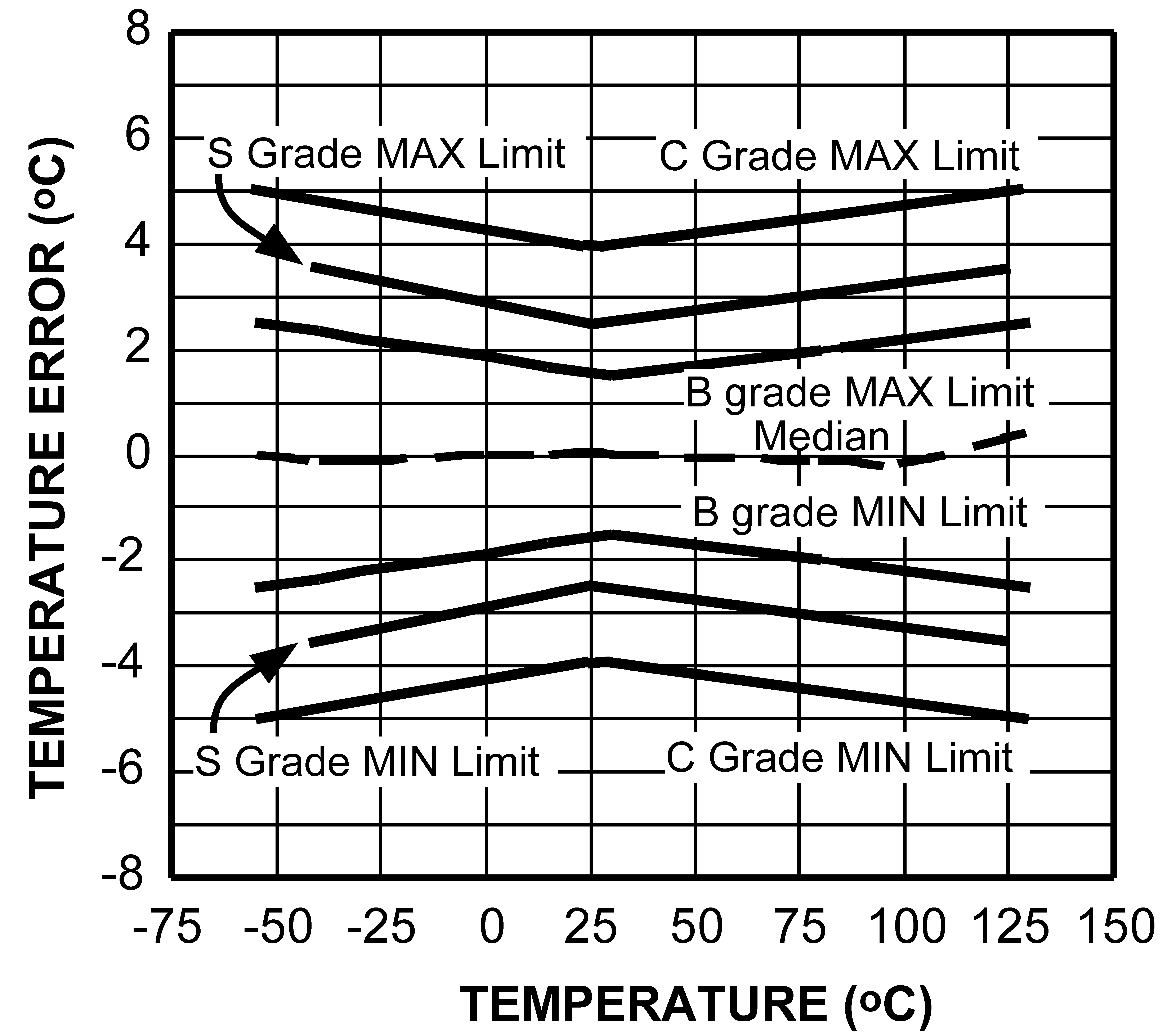 Figure 1. Temperature Error vs Temperature