SNLS384G February   1995  – June 2015 LM1881

PRODUCTION DATA.  

  1. Features
  2. Applications
  3. Description
  4. Revision History
  5. Pin Configuration and Functions
  6. Specifications
    1. 6.1 Absolute Maximum Ratings
    2. 6.2 ESD Ratings
    3. 6.3 Recommended Operating Conditions
    4. 6.4 Electrical Characteristics LM1881
    5. 6.5 Dissipation Ratings
    6. 6.6 Typical Characteristics
  7. Detailed Description
    1. 7.1 Overview
    2. 7.2 Functional Block Diagram
    3. 7.3 Feature Description
      1. 7.3.1 Composite Sync Output
      2. 7.3.2 Vertical Sync Output
      3. 7.3.3 Odd and Even Field Pulse
      4. 7.3.4 Burst or Back Porch Output Pulse
    4. 7.4 Device Functional Modes
      1. 7.4.1 Operation Mode
  8. Application and Implementation
    1. 8.1 Application Information
    2. 8.2 Typical Applications
      1. 8.2.1 Video Line Selector
        1. 8.2.1.1 Design Requirements
        2. 8.2.1.2 Detailed Design Procedure
      2. 8.2.2 Multiple Contiguous Video Line Selector With Black Level Restoration
        1. 8.2.2.1 Design Requirements
        2. 8.2.2.2 Detailed Design Procedure
  9. Power Supply Recommendations
  10. 10Device and Documentation Support
    1. 10.1 Community Resources
    2. 10.2 Trademarks
    3. 10.3 Electrostatic Discharge Caution
    4. 10.4 Glossary
  11. 11Mechanical, Packaging, and Orderable Information

封装选项

机械数据 (封装 | 引脚)
散热焊盘机械数据 (封装 | 引脚)
订购信息

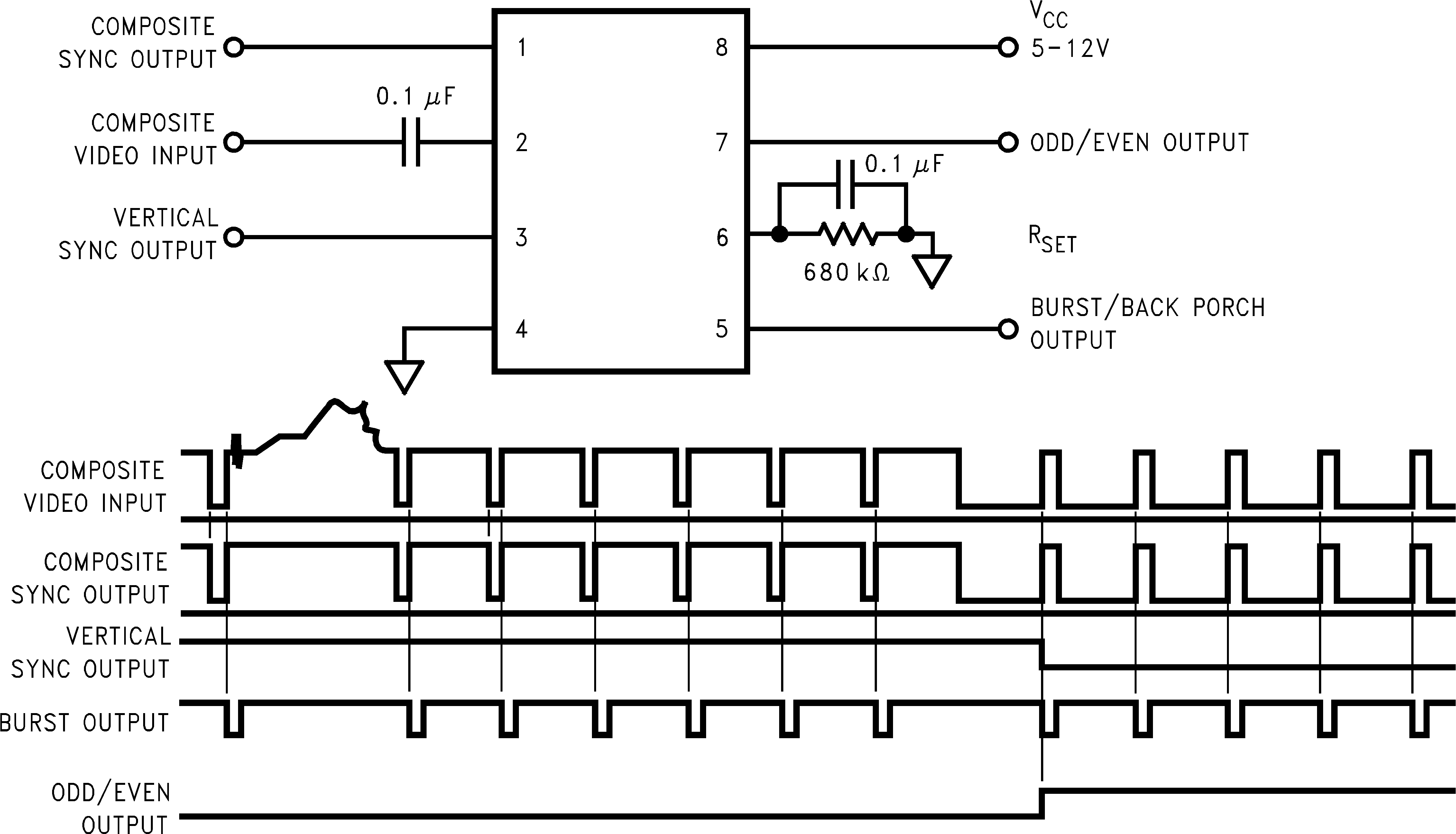
5 Pin Configuration and Functions

D and P Packages
8-Pin SOIC and PDIP
Top View
LM1881 00915001.png

Pin Functions

PIN TYPE DESCRIPTION
NO. NAME
1 CSOUT Output Composite Sync Output
2 CVIN Input Composite Video Input
3 VSOUT Output Vertical Sync Output
4 GND Ground
5 BPOUT Output Burst or Back Porch Timing Output
6 RSET Input Charge Current External Resistor
7 OEOUT Output Odd and Even Field Output
8 VCC Input Supply Voltage