SNVS739F December 2011 – October 2016 LM10504
PRODUCTION DATA.
- 1 Features
- 2 Applications
- 3 Description
- 4 Revision History
- 5 Pin Configuration and Functions
-
6 Specifications
- 6.1 Absolute Maximum Ratings
- 6.2 ESD Ratings
- 6.3 Recommended Operating Conditions
- 6.4 Thermal Information
- 6.5 Electrical Characteristics - General
- 6.6 Electrical Characteristics - Buck 1
- 6.7 Electrical Characteristics - Buck 2
- 6.8 Electrical Characteristics - Buck 3
- 6.9 Electrical Characteristics - LDO
- 6.10 Electrical Characteristics - Comparators
- 6.11 Typical Characteristics
-
7 Detailed Description
- 7.1 Overview
- 7.2 Functional Block Diagram
- 7.3 Feature Description
- 7.4
Device Functional Modes
- 7.4.1 Start-Up Sequence
- 7.4.2 Power-On Default and Device Enable
- 7.4.3 Reset Pin Function
- 7.4.4 DevSLP Function
- 7.4.5 Vselect_B2, Vselect_B3 Function
- 7.4.6 Undervoltage Lockout (UVLO)
- 7.4.7 Overvoltage Lockout (OVLO)
- 7.4.8 Device Status, Interrupt Enable
- 7.4.9 Thermal Shutdown (TSD)
- 7.4.10 Comparator
- 7.5 Programming
- 7.6 Register Maps
-
8 Application and Implementation
- 8.1 Application Information
- 8.2
Typical Application
- 8.2.1 Design Requirements
- 8.2.2 Detailed Design Procedure
- 8.2.3 Application Curves
- 9 Power Supply Recommendations
- 10Layout
- 11Device and Documentation Support
- 12Mechanical, Packaging, and Orderable Information
6 Specifications
6.1 Absolute Maximum Ratings
over operating free-air temperature range (unless otherwise noted)(1)(2)| MIN | MAX | UNIT | ||
|---|---|---|---|---|
| VIN, VCOMP | –0.3 | 6 | V | |
| VIN_IO, VIN_B1, VIN_B2, VIN_B3, SPI_CS, SPI_DI, SPI_CLK, SPI_DO, Vselect_B2,Vselect_B3, RESET, SW_1, SW_2, SW_3, FB_1, FB_2, FB_3, LDO, Interrupt, DevSLP | –0.3 | 6 | V | |
| Junction temperature, TJ-MAX | 150 | °C | ||
| Storage temperature, Tstg | –65 | 150 | °C | |
(1) Stresses beyond those listed under Absolute Maximum Ratings may cause permanent damage to the device. These are stress ratings only, which do not imply functional operation of the device at these or any other conditions beyond those indicated under Recommended Operating Conditions. Exposure to absolute-maximum-rated conditions for extended periods may affect device reliability.
(2) If Military/Aerospace specified devices are required, please contact the TI Sales Office/Distributors for availability and specifications.
6.2 ESD Ratings
| VALUE | UNIT | |||
|---|---|---|---|---|
| V(ESD) | Electrostatic discharge | Human-body model (HBM), per ANSI/ESDA/JEDEC JS-001(1) | ±2000 | V |
(1) JEDEC document JEP155 states that 500-V HBM allows safe manufacturing with a standard ESD control process.
6.3 Recommended Operating Conditions
over operating free-air temperature range (unless otherwise noted)(1)(2)(3)| MIN | MAX | UNIT | ||
|---|---|---|---|---|
| VIN_B1, VIN_B2_VIN_B3, VIN | 3 | 5.5 | V | |
| VIN_IO | 1.72 | 3.63 | V | |
| All pins other than VIN_IO | 0 | VIN | V | |
| PD-MAX | Maximum continuous power dissipation | 0.9 | W | |
| TA | Ambient temperature | –30 | 85 | °C |
| TJ | Junction temperature | –30 | 125 | °C |
(1) Internal thermal shutdown protects device from permanent damage. Thermal shutdown engages at TJ = 140°C and disengages at
TJ = 120°C (typically). Thermal shutdown is ensured by design.
TJ = 120°C (typically). Thermal shutdown is ensured by design.
(2) In applications where high power dissipation or poor thermal resistance is present, the maximum ambient temperature may have to be derated. Maximum ambient temperature (TA-MAX) is dependent on the maximum operating junction temperature (TJ-MAX-OP = 125°C), the maximum power dissipation of the device in the application (PD-MAX), and the junction-to-ambient thermal resistance of the part or package in the application (RθJA), as given by the following equation: TA-MAX = TJ-MAX-OP – (RθJA × PD-MAX).
(3) The amount of absolute maximum power dissipation allowed for the device depends on the ambient temperature and can be calculated using the formula: P = (TJ – TA) / RθJA, where TJ is the junction temperature, TA is the ambient temperature, and RθJA is the junction-to-ambient thermal resistance. RθJA is highly application and board-layout dependent. Internal thermal shutdown circuitry protects the device from permanent damage (see Electrical Characteristics – General).
6.4 Thermal Information
| THERMAL METRIC(1) | LM10504 | UNIT | |
|---|---|---|---|
| YFR (DSBGA) | |||
| 34 PINS | |||
| RθJA | Junction-to-ambient thermal resistance | 65.6 | °C/W |
| RθJC(top) | Junction-to-case (top) thermal resistance | 0.2 | °C/W |
| RθJB | Junction-to-board thermal resistance | 39 | °C/W |
| ψJT | Junction-to-top characterization parameter | 1.5 | °C/W |
| ψJB | Junction-to-board characterization parameter | 38.6 | °C/W |
| RθJC(bot) | Junction-to-case (bottom) thermal resistance | — | °C/W |
(1) For more information about traditional and new thermal metrics, see the Semiconductor and IC Package Thermal Metrics application report.
6.5 Electrical Characteristics – General
TJ = 25°C and VIN = 5 V where VIN = VIN_B1 = VIN_B2 = VIN_B3 (unless otherwise noted)(1)(2)| PARAMETER | TEST CONDITIONS | MIN | TYP | MAX | UNIT | ||
|---|---|---|---|---|---|---|---|
| IQ(DEVSLP) | Quiescent supply current | DevSLP = HIGH, no load |
TJ = 25°C | 100 | µA | ||
| –30°C ≤ TJ ≤ 85°C | 200 | ||||||
| UNDERVOLTAGE OR OVERVOLTAGE LOCKOUT | |||||||
| VUVLO_RISING | Undervoltage lockout, rising | TJ = 25°C | 2.9 | V | |||
| –30°C ≤ TJ ≤ 85°C | 2.75 | 3.05 | |||||
| VUVLO_FALLING | Undervoltage lockout, falling | TJ = 25°C | 2.6 | V | |||
| –30°C ≤ TJ ≤ 85°C | 2.45 | 2.75 | |||||
| VOVLO_RISING | Overvoltage lockout, rising | 5.64 | V | ||||
| VOVLO_FALLING | Overvoltage lockout, falling | 5.54 | V | ||||
| DIGITAL INTERFACE | |||||||
| VIL | Logic input low | SPI_CS, SPI_DI, SPI_CLK, RESET, DevSLP, –30°C ≤ TJ ≤ 85°C |
0.7 × VIN_IO | 0.3 × VIN_IO | V | ||
| VIH | Logic input high | SPI_CS, SPI_DI, SPI_CLK, RESET, DevSLP, –30°C ≤ TJ ≤ 85°C |
|||||
| VIL | Logic input low | Vselect_B2, Vselect_B3, –30°C ≤ TJ ≤ 85°C |
0.7 × VIN | 0.3 × VIN | V | ||
| VIH | Logic input high | Vselect_B2, Vselect_B3, –30°C ≤ TJ ≤ 85°C |
|||||
| VOL | Logic output low | SPI_DO, –30°C ≤ TJ ≤ 85°C | 0.8 × VIN_IO | 0.2 × VIN_IO | V | ||
| VOH | Logic output high | SPI_DO, –30°C ≤ TJ ≤ 85°C | |||||
| IIL | Input current, pin driven low | SPI_CS, SPI_DI, SPI_CLK, Vselect_B2, DevSLP | –2 | µA | |||
| Vselect_B3, RESET | –5 | ||||||
| IIH | Input current, pin driven high | SPI_CS, SPI_DI, SPI_CLK, Vselect_B3, RESET | 2 | µA | |||
| Vselect_B2, DevSLP | 5 | ||||||
| fSPI_MAX | SPI max frequency | –30°C ≤ TJ ≤ 85°C | 10 | MHz | |||
| tRESET | Minimum pulse width(3) | –30°C ≤ TJ ≤ 85°C | 2 | µs | |||
| tDEVSLP | |||||||
(1) All limits are ensured by design, test, or statistical analysis. All electrical characteristics having room-temperature limits are tested during production with TJ = 25°C. All hot and cold limits are ensured by correlating the electrical characteristics to process and temperature variations and applying statistical process control.
(2) Capacitors: Low-ESR surface-mount ceramic capacitors (MLCCs) are used in setting electrical characteristics.
(3) Specification ensured by design. Not tested during production.
6.6 Electrical Characteristics – Buck 1
TJ = 25°C and VIN = 5 V where VIN=VIN_B1 = VIN_B2 = VIN_B3 (unless otherwise noted)(1)(2)(3)| PARAMETER | CONDITIONS | MIN | TYP | MAX | UNITS | ||
|---|---|---|---|---|---|---|---|
| IQ | VIN DC bias current | No load, PFM mode | TJ = 25°C | 15 | µA | ||
| –30°C ≤ TJ ≤ 85°C | 50 | ||||||
| IOUT_MAX | Continuous maximum load current(4)(5) | Buck 1 enabled, switching in PWM, –30°C ≤ TJ ≤ 85°C |
1.6 | A | |||
| IPEAK | Peak switching current limit | Buck 1 enabled, switching in PWM | TJ = 25°C | 2.1 | A | ||
| –30°C ≤ TJ ≤ 85°C | 1.9 | 2.6 | |||||
| η | Peak efficiency(4) | IOUT = 0.3 A | 90% | ||||
| FSW | Switching frequency | TJ = 25°C | 2 | MHz | |||
| –30°C ≤ TJ ≤ 85°C | 1.75 | 2.3 | |||||
| CIN | Input capacitor(4) | 0 mA ≤ IOUT ≤ IOUT-MAX | 4.7 | µF | |||
| COUT | Output filter capacitor(4) | 0 mA ≤ IOUT ≤ IOUT-MAX | 10 | 10 | 100 | ||
| Output capacitor ESR(4) | 0 mA ≤ IOUT ≤ IOUT-MAX | 20 | mΩ | ||||
| L | Output filter inductance(4) | 0 mA ≤ IOUT ≤ IOUT-MAX | 2.2 | µH | |||
| ΔVOUT | DC line regulation(4) | 3.3 V ≤ VIN ≤ 5 V, IOUT = IOUT-MAX | 0.5% | V | |||
| DC load regulation(4) | 100 mA ≤ IOUT ≤ IOUT-MAX | 0.3% | A | ||||
| IFB | Feedback pin input bias current | VFB = 3 V | TJ = 25°C | 2.1 | µA | ||
| –30°C ≤ TJ ≤ 85°C | 5 | ||||||
| RDS-ON-HS | High-side switch on resistance | 135 | mΩ | ||||
| VIN = 2.6 V | 215 | ||||||
| RDS-ON-LS | Low-side switch on resistance | TJ = 25°C | 85 | mΩ | |||
| –30°C ≤ TJ ≤ 85°C | 190 | ||||||
| RDS-ON-BYPASS | Bypass FET on resistance | Used in parallel with the high-side FET while in bypass mode. Resistance (DCR) of inductor = 100 mΩ |
|||||
| VIN = 3.3 V | 85 | mΩ | |||||
| VIN = 2.6 V | 120 | ||||||
| START-UP | |||||||
| TSTART | Internal soft-start (turnon time)(4) | Start up from shutdown, VOUT = 0 V, no load, LC = recommended circuit, using software enable, to VOUT = 95% of final value |
0.1 | ms | |||
(1) All limits are ensured by design, test, or statistical analysis. All electrical characteristics having room-temperature limits are tested during production with TJ = 25°C. All hot and cold limits are ensured by correlating the electrical characteristics to process and temperature variations and applying statistical process control.
(2) Capacitors: Low-ESR surface-mount ceramic capacitors (MLCCs) are used in setting electrical characteristics.
(3) BUCK normal operation is ensured if VIN ≥ VOUT + 1 V.
(4) Specification ensured by design. Not tested during production.
(5) In applications where high power dissipation or poor thermal resistance is present, the maximum ambient temperature may have to be derated. Maximum ambient temperature (TA-MAX) is dependent on the maximum operating junction temperature (TJ-MAX-OP = 125°C), the maximum power dissipation of the device in the application (PD-MAX), and the junction-to-ambient thermal resistance of the part or package in the application (RθJA), as given by the following equation: TA-MAX = TJ-MAX-OP – (RθJA × PD-MAX).
6.7 Electrical Characteristics – Buck 2
TJ = 25°C and VIN = 5 V where VIN=VIN_B1 = VIN_B2 = VIN_B3 (unless otherwise noted)(1)(2)(3)| PARAMETER | TEST CONDITIONS | MIN | TYP | MAX | UNIT | ||
|---|---|---|---|---|---|---|---|
| IQ | VIN DC bias current | No load, PFM mode | TJ = 25°C | 15 | µA | ||
| –30°C ≤ TJ ≤ 85°C | 50 | ||||||
| IOUT_MAX | Continuous maximum load current(4)(5) | Buck 2 enabled, switching in PWM, –30°C ≤ TJ ≤ 85°C |
1 | A | |||
| IPEAK | Peak switching current limit | Buck 2 enabled, switching in PWM | TJ = 25°C | 1.56 | A | ||
| –30°C ≤ TJ ≤ 85°C | 1.35 | 1.8 | |||||
| η | Peak efficiency(4) | IOUT = 0.3 A | 90% | ||||
| FSW | Switching frequency | TJ = 25°C | 2 | MHz | |||
| –30°C ≤ TJ ≤ 85°C | 1.75 | 2.3 | |||||
| CIN | Input capacitor(4) | 0 mA ≤ IOUT ≤ IOUT-MAX | 4.7 | µF | |||
| COUT | Output filter capacitor(4) | 0 mA ≤ IOUT ≤ IOUT-MAX | 10 | 10 | 100 | ||
| Output capacitor ESR(4) | 0 mA ≤ IOUT ≤ IOUT-MAX | 20 | mΩ | ||||
| L | Output filter inductance(4) | 0 mA ≤ IOUT ≤ IOUT-MAX | 2.2 | µH | |||
| ΔVOUT | DC line regulation(4) | 3.3 V ≤ VIN ≤ 5 V, IOUT = IOUT-MAX | 0.5% | V | |||
| DC load regulation(4) | 100 mA ≤ IOUT ≤ IOUT-MAX | 0.3% | A | ||||
| IFB | Feedback pin input bias current | VFB = 1.8 V | TJ = 25°C | 1.8 | µA | ||
| –30°C ≤ TJ ≤ 85°C | 5 | ||||||
| RDS-ON-HS | High-side switch on resistance | 135 | mΩ | ||||
| VIN = 2.6 V | 260 | ||||||
| RDS-ON-LS | Low-side switch on resistance | TJ = 25°C | 85 | ||||
| –30°C ≤ TJ ≤ 85°C | 190 | ||||||
| START-UP | |||||||
| TSTART | Internal soft-start (turnon time)(4) | Start up from shutdown, VOUT = 0 V, no load, LC = recommended circuit, using software enable, to VOUT = 95% of final value |
0.1 | ms | |||
(1) All limits are ensured by design, test, or statistical analysis. All electrical characteristics having room-temperature limits are tested during production with TJ = 25°C. All hot and cold limits are ensured by correlating the electrical characteristics to process and temperature variations and applying statistical process control.
(2) Capacitors: Low-ESR surface-mount ceramic capacitors (MLCCs) are used in setting electrical characteristics.
(3) BUCK normal operation is ensured if VIN ≥ VOUT + 1 V.
(4) Specification ensured by design. Not tested during production.
(5) In applications where high power dissipation or poor thermal resistance is present, the maximum ambient temperature may have to be derated. Maximum ambient temperature (TA-MAX) is dependent on the maximum operating junction temperature (TJ-MAX-OP = 125°C), the maximum power dissipation of the device in the application (PD-MAX), and the junction-to-ambient thermal resistance of the part or package in the application (RθJA), as given by the following equation: TA-MAX = TJ-MAX-OP – (RθJA × PD-MAX).
6.8 Electrical Characteristics – Buck 3
TJ = 25°C and VIN = 5 V where VIN = VIN_B1 = VIN_B2 = VIN_B3 (unless otherwise noted)(1)(2)(3)| PARAMETER | TEST CONDITIONS | MIN | TYP | MAX | UNIT | ||
|---|---|---|---|---|---|---|---|
| IQ | VIN DC bias current | No load, PFM mode | TJ = 25°C | 15 | µA | ||
| –30°C ≤ TJ ≤ 85°C | 50 | ||||||
| IOUT_MAX | Continuous maximum load current(4)(5) | Buck 3 enabled, switching in PWM, –30°C ≤ TJ ≤ 85°C |
1 | A | |||
| IPEAK | Peak switching current limit | Buck 3 enabled, switching in PWM | TJ = 25°C | 1.56 | A | ||
| –30°C ≤ TJ ≤ 85°C | 1.35 | 1.8 | |||||
| η | Peak efficiency(4) | IOUT = 0.3 A | 90% | ||||
| FSW | Switching frequency | TJ = 25°C | 2 | MHz | |||
| –30°C ≤ TJ ≤ 85°C | 1.75 | 2.3 | |||||
| CIN | Input capacitor(4) | 0 mA ≤ IOUT ≤ IOUT-MAX | 4.7 | µF | |||
| COUT | Output filter capacitor(4) | 0 mA ≤ IOUT ≤ IOUT-MAX | 10 | 10 | 100 | ||
| Output capacitor ESR(4) | 0 mA ≤ IOUT ≤ IOUT-MAX | 20 | mΩ | ||||
| L | Output filter inductance(4) | 0 mA ≤ IOUT ≤ IOUT-MAX | 2.2 | µH | |||
| ΔVOUT | DC line regulation(4) | 3.3 V ≤ VIN ≤ 5 V, IOUT = IOUT-MAX | 0.5% | V | |||
| DC load regulation(4) | 100 mA ≤ IOUT ≤ IOUT-MAX | 0.3% | A | ||||
| IFB | Feedback pin input bias current | VFB = 1.2 V | TJ = 25°C | 0.9 | µA | ||
| –30°C ≤ TJ ≤ 85°C | 5 | ||||||
| RDS-ON-HS | High-side switch on resistance | 135 | mΩ | ||||
| VIN = 2.6 V | 260 | ||||||
| RDS-ON-LS | Low-side switch on resistance | TJ = 25°C | 85 | ||||
| –30°C ≤ TJ ≤ 85°C | 190 | ||||||
| START-UP | |||||||
| TSTART | Internal soft-start (turnon time)(4) | Start up from shutdown, VOUT = 0 V, no load, LC = recommended circuit, using software enable, to VOUT = 95% of final value | 0.1 | ms | |||
(1) All limits are ensured by design, test, or statistical analysis. All electrical characteristics having room-temperature limits are tested during production with TJ = 25°C. All hot and cold limits are ensured by correlating the electrical characteristics to process and temperature variations and applying statistical process control.
(2) Capacitors: Low-ESR surface-mount ceramic capacitors (MLCCs) are used in setting electrical characteristics.
(3) BUCK normal operation is ensured if VIN ≥ VOUT + 1 V.
(4) Specification ensured by design. Not tested during production.
(5) In applications where high power dissipation or poor thermal resistance is present, the maximum ambient temperature may have to be derated. Maximum ambient temperature (TA-MAX) is dependent on the maximum operating junction temperature (TJ-MAX-OP = 125°C), the maximum power dissipation of the device in the application (PD-MAX), and the junction-to-ambient thermal resistance of the part or package in the application (RθJA), as given by the following equation: TA-MAX = TJ-MAX-OP – (RθJA × PD-MAX).
6.9 Electrical Characteristics – LDO
TJ = 25°C and VIN = 5 V where: VIN = VIN_B1 = VIN_B2 = VIN_B3 (unless otherwise noted)(1)(2)| PARAMETER | TEST CONDITIONS | MIN | TYP | MAX | UNIT | ||
|---|---|---|---|---|---|---|---|
| VOUT | Output voltage accuracy | IOUT = 1 mA, –30°C ≤ TJ ≤ 85°C | –3% | 3% | |||
| IOUT | Maximum output current | 250 | mA | ||||
| ISC | Short-circuit current limit | VOUT = 0 V | 0.5 | A | |||
| VDO | Dropout voltage | IOUT = 250 mA | TJ = 25°C | 160 | mV | ||
| –30°C ≤ TJ ≤ 85°C | 220 | ||||||
| ΔVOUT | Line regulation | 3.3 V ≤ VIN ≤ 5 V, IOUT = 1 mA | 5 | ||||
| Load regulation | 1 mA ≤ IOUT ≤ 250 mA, VIN = 3.3 V, 5 V | 5 | |||||
| eN | Output noise voltage(3) | 10 Hz ≤ f ≤ 100 kHz | VIN = 5 V | 10 | µVRMS | ||
| VIN = 3.3 V | 35 | ||||||
| PSRR | Power supply rejection ratio(3) | F = 10 kHz, COUT = 4.7 µF, IOUT = 20 mA | VIN = 5 V | 65 | dB | ||
| VIN = 3.3 V | 40 | ||||||
| TSTART | Start-up time from shutdown(3) | COUT = 4.7 µF, IOUT = 250 mA | VIN = 5 V | 45 | µs | ||
| VIN = 3.3 V | 60 | ||||||
| TTRANSIENT | Start-up transient overshoot(3) | COUT = 4.7 µF, IOUT = 250 mA, –30°C ≤ TJ ≤ 85°C | 30 | mV | |||
(1) All limits are ensured by design, test, or statistical analysis. All electrical characteristics having room-temperature limits are tested during production with TJ = 25°C. All hot and cold limits are ensured by correlating the electrical characteristics to process and temperature variations and applying statistical process control.
(2) Capacitors: Low-ESR surface-mount ceramic capacitors (MLCCs) are used in setting electrical characteristics.
(3) Specification ensured by design. Not tested during production.
6.10 Electrical Characteristics – Comparators
TJ = 25°C and VIN = 5 V (unless otherwise noted)(1)(2)| PARAMETER | TEST CONDITIONS | MIN | TYP | MAX | UNIT | ||
|---|---|---|---|---|---|---|---|
| IVCOMP | VCOMP pin bias current | VCOMP = 0 V | TJ = 25°C | 0.1 | µA | ||
| –30°C ≤ TJ ≤ 85°C | 2 | ||||||
| VCOMP = 5 V | TJ = 25°C | 0.1 | |||||
| –30°C ≤ TJ ≤ 85°C | 2 | ||||||
| VCOMP_RISE | Comparator rising edge trigger level | 2.79 | V | ||||
| VCOMP_FALL | Comparator falling edge trigger level | 2.74 | |||||
| Hysteresis | TJ = 25°C | 60 | mV | ||||
| –30°C ≤ TJ ≤ 85°C | 30 | 80 | |||||
| InterruptVOH | Output voltage high | –30°C ≤ TJ ≤ 85°C | 0.8 × VIN_IO | V | |||
| InterruptVOL | Output voltage low | –30°C ≤ TJ ≤ 85°C | 0.2 × VIN_IO | ||||
| tCOMP | Transition time of interrupt output | TJ = 25°C | 6 | µs | |||
| –30°C ≤ TJ ≤ 85°C | 15 | ||||||
(1) All limits are ensured by design, test, or statistical analysis. All electrical characteristics having room-temperature limits are tested during production with TJ = 25°C. All hot and cold limits are ensured by correlating the electrical characteristics to process and temperature variations and applying statistical process control.
(2) Capacitors: Low-ESR surface-mount ceramic capacitors (MLCCs) are used in setting electrical characteristics.
6.11 Typical Characteristics
TA = 25°C (unless otherwise noted)
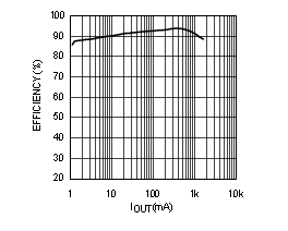
| VIN= 5 V | VOUT = 3 V |
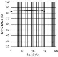
| VIN = 5 V | VOUT = 1 V |
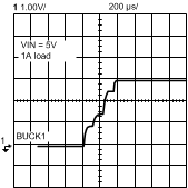
| VIN = 5 V | VOUT = 3 V |
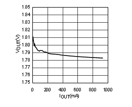
| VIN = 5 V | VOUT = 1.8 V |
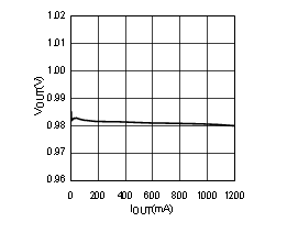
| VIN = 5 V | VOUT = 1 V |
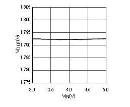
| VOUT = 1.8 V | IOUT = 1 A |
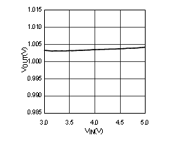
| VOUT= 1 V | IOUT= 1 A |
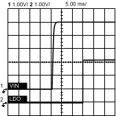
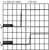
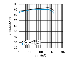
| VIN = 5 V |
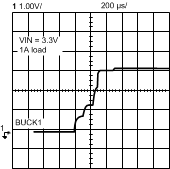
| VIN = 3.3 V | VOUT = 3 V |
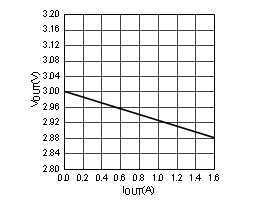
| VIN = 5 V | VOUT = 3 V |
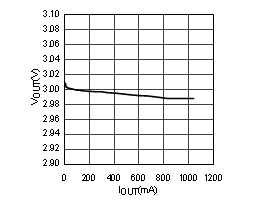
| VIN = 5 V | VOUT = 3 V |
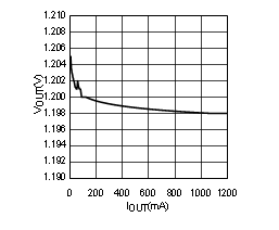
| VIN = 5 V | VOUT = 1.2 V |
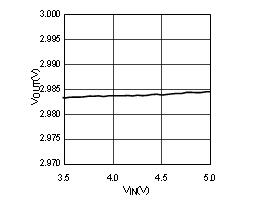
| VOUT = 3 V | IOUT= 1 A |
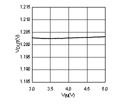
| VOUT= 1.2 V | IOUT = 1 A |
