SBOS562G August 2011 – June 2020 INA826
PRODUCTION DATA.
- 1 Features
- 2 Applications
- 3 Description
- 4 Revision History
- 5 Device Comparison Table
- 6 Pin Configuration and Functions
- 7 Specifications
-
8 Detailed Description
- 8.1 Overview
- 8.2 Functional Block Diagram
- 8.3 Feature Description
- 8.4 Device Functional Modes
- 9 Application and Implementation
- 10Power Supply Recommendations
- 11Layout
- 12Device and Documentation Support
- 13Mechanical, Packaging, and Orderable Information
封装选项
机械数据 (封装 | 引脚)
散热焊盘机械数据 (封装 | 引脚)
- DRG|8
订购信息
9.3.3 Using TINA-TI SPICE-Based Analog Simulation Program With the INA826
TINA is a simple, powerful, and easy-to-use circuit simulation program based on a SPICE engine. TINA-TI is a free, fully-functional version of the TINA software, preloaded with a library of macromodels in addition to a range of both passive and active models. TINA provides all the conventional dc, transient, and frequency domain analysis of SPICE as well as additional design capabilities.
Available as a free download from the Analog eLab Design Center, TINA-TI offers extensive post-processing capability that allows users to format results in a variety of ways. Virtual instruments offer users the ability to select input waveforms and probe circuit nodes, voltages, and waveforms, creating a dynamic quick-start tool.
Figure 68 and Figure 70 illustrate example TINA-TI circuits for the INA826 that can be used to develop, modify, and assess the circuit design for specific applications. Links to download these simulation files are provided in this section.
NOTE
These files require that either the TINA software (from DesignSoft) or TINA-TI software be installed. Download the free TINA-TI software from the TINA-TI folder.
The circuit in Figure 68 is used to convert inputs of ±10 V, ±5 V, or ±20 mA to an output voltage range from 0.5 V to 4.5 V. The input selection depends on the settings of SW1 and SW2. Further explanation as well as the TINA-TI simulation circuit is provided in the compressed file that can be downloaded at the following link: PLC Circuit.
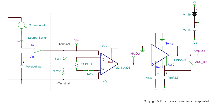 Figure 68. Two-Terminal Programmable Logic Controller (PLC) Input
 Figure 69 is an example of a LEAD I ECG circuit. The input signals come from leads attached to the right arm (RA) and left arm (LA). These signals are simulated with the circuitry in the corresponding boxes. Protection resistors (RPROT1 and RPROT2) and filtering are also provided. The OPA333 is used as an integrator to remove the gained-up dc offsets and servo the INA826 outputs to VREF. Finally, the right leg drive is biased to a potential (+VS / 2), and inverts and amplifies the average common-mode signal back into the patient's right leg. This architecture reduces the 50-Hz and 60-Hz noise pickup.
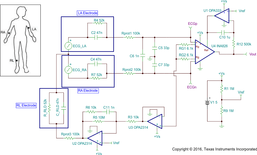 Figure 69. ECG Circuit
 Figure 70 shows an example of how the INA826 can be used for low-side current sensing. The load current (ILOAD) creates a voltage drop across the shunt resistor (RSHUNT). This voltage is amplified by the INA826 with gain set to 100. The output swing of the INA826 is set by the common-mode voltage (which is 0 V in low-side current sensing) and power supplies. Therefore, a dual-supply circuit is implemented. The load current is set from 1 A to 10 A, corresponding to an output voltage range from 350 mV to 3.5 V. The output range can be adjusted by changing the shunt resistor and the gain of the INA826. Click the following link to download the TINA-TI file: Current Sensing Circuit.
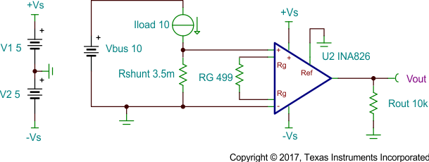 Figure 70. Low-Side Current Sensing
 Figure 71 shows an example of how the INA826 can be used for RTD signal conditioning. This circuit creates an excitation current (ISET) by forcing 2.5 V from the REF5025 across RSET. The zero-drift, low-noise OPA188 creates the virtual ground that maintains a constant differential voltage across RSET with changing common-mode voltage. This voltage is necessary because the voltage on the positive input of the INA826 fluctuates over temperature as a result of the changing RTD resistance. Click the following link to download the TINA-TI file: RTD Circuit.
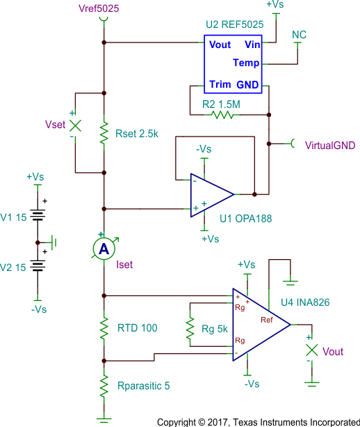 Figure 71. RTD Signal Conditioning
 The circuit in Figure 72 creates a precision current ISET by forcing the INA826 VDIFF across RSET. The input voltage VIN is amplified to the output of the INA826 and then divided down by the gain of the INA826 to create VDIFF. ISET can be controlled either by changing the value of the gain-set resistor RG, the set resistor RSET, or by changing VOUT through the gain of the composite loop. Make sure that the changing load resistance RL does not create a voltage on the negative input of the INA826 that violates the compliance of the common-mode input range. Likewise, the voltage on the output of the OPA170 must remain compliant throughout the changing load resistance for this circuit to function properly.
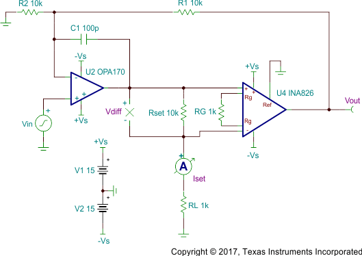 Figure 72. Precision Current Source