ZHCSAK0C July 2008 – December 2015 INA333
PRODUCTION DATA.
- 1 特性
- 2 应用范围
- 3 说明
- 4 修订历史记录
- 5 Pin Configuration and Functions
- 6 Specifications
- 7 Detailed Description
- 8 Application and Implementation
- 9 Power Supply Recommendations
- 10Layout
- 11器件和文档支持
- 12机械、封装和可订购信息
封装选项
机械数据 (封装 | 引脚)
散热焊盘机械数据 (封装 | 引脚)
- DRG|8
订购信息
7 Detailed Description
7.1 Overview
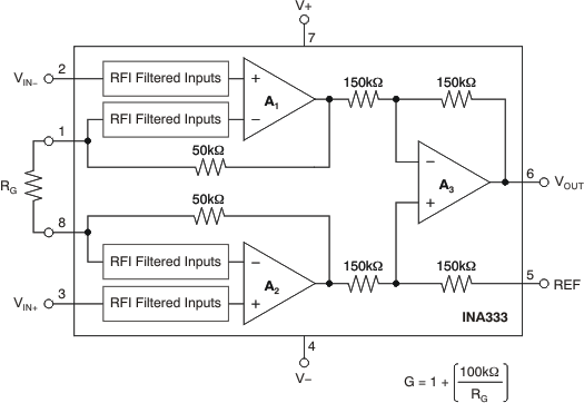
The INA333 is a monolithic instrumentation amplifier (INA) based on the precision zero-drift OPA333 (operational amplifier) core. The INA333 also integrates laser-trimmed resistors to ensure excellent common-mode rejection and low gain error. The combination of the zero-drift amplifier core and the precision resistors allows this device to achieve outstanding DC precision and makes the INA333 ideal for many 3.3-V and 5-V industrial applications.
7.2 Functional Block Diagram

7.3 Feature Description
The INA333 is a low-power, zero-drift instrumentation amplifier offering excellent accuracy. The versatile three-operational-amplifier design and small size make the amplifiers ideal for a wide range of applications. Zero-drift chopper circuitry provides excellent DC specifications. A single external resistor sets any gain from 1 to 10,000. The INA333 is laser trimmed for very high common-mode rejection (100 dB at G ≥ 100). This devices operate with power supplies as low as 1.8 V, and quiescent current of 50 µA, typically.
7.4 Device Functional Modes
7.4.1 Internal Offset Correction
INA333 internal operational amplifiers use an auto-calibration technique with a time-continuous 350-kHz operational amplifier in the signal path. The amplifier is zero-corrected every 8 µs using a proprietary technique. Upon power up, the amplifier requires approximately 100 µs to achieve specified VOS accuracy. This design has no aliasing or flicker noise.
7.4.2 Input Common-Mode Range
The linear input voltage range of the input circuitry of the INA333 is from approximately 0.1 V below the positive supply voltage to 0.1 V above the negative supply. As a differential input voltage causes the output voltage to increase, however, the linear input range is limited by the output voltage swing of amplifiers A1 and A2. Thus, the linear common-mode input range is related to the output voltage of the complete amplifier. This behavior also depends on supply voltage—see Figure 20.
Input overload conditions can produce an output voltage that appears normal. For example, if an input overload condition drives both input amplifiers to the respective positive output swing limit, the difference voltage measured by the output amplifier is near zero. The output of the INA333 is near 0 V even though both inputs are overloaded.