ZHCSC46C February 2014 – June 2021 INA300
PRODUCTION DATA
- 1 特性
- 2 应用
- 3 说明
- 4 Revision History
- 5 Pin Configuration and Functions
- 6 Specifications
-
7 Detailed Description
- 7.1 Overview
- 7.2 Functional Block Diagram
- 7.3 Feature Description
- 7.4 Device Functional Modes
- 8 Application and Implementation
- 9 Power Supply Recommendations
- 10Layout
- 11Device and Documentation Support
- 12Mechanical, Packaging, and Orderable Information
7.3.4 Alert Timing Response
The device has a 10-µs internal comparison window where the input signal is measured to compare to the limit threshold voltage. This window continuously runs internal to the device without any external indicator or control. A comparison is made at the completion of each 10-µs comparison window to determine if the averaged input over the comparison window exceeds the limit threshold, thus indicating if an overcurrent event has occurred.
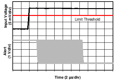
This comparison window is not synchronized with the input signal so there is an unknown timing component present. With this free-running internal timing window, an overcurrent event can occur anywhere within the 10-µs comparison window. This condition causes a variation in the amount of time before the alert appears at the output because the comparison is always made at the end of the 10-µs comparison window. Figure 7-3 shows the variation in time between when the input signal rises above the threshold voltage and when a change at the alert output terminal occurs.
 Figure 7-3 10-µs Alert Response Window
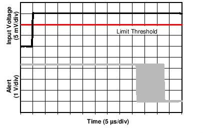
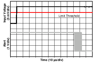
The delay shown in Figure 7-3 represents the response time of the device with a 10-µs delay setting. With a
50-µs delay setting, an additional 40 µs is added to the timing response, as shown in Figure 7-4. A 100-µs delay setting adds 90 µs to the response time, as shown in Figure 7-5.
 Figure 7-4 50-µs Alert Response Window
 Figure 7-5 100-µs Alert Response Window