SBOS401C July   2007  – April 2016 INA270A-Q1 , INA271A-Q1

PRODUCTION DATA.  

  1. Features
  2. Applications
  3. Description
  4. Revision History
  5. Device Comparison Table
  6. Pin Configuration and Functions
  7. Specifications
    1. 7.1 Absolute Maximum Ratings
    2. 7.2 ESD Ratings
    3. 7.3 Recommended Operating Conditions
    4. 7.4 Thermal Information
    5. 7.5 Electrical Characteristics
    6. 7.6 Typical Characteristics
  8. Detailed Description
    1. 8.1 Overview
    2. 8.2 Functional Block Diagram
    3. 8.3 Feature Description
      1. 8.3.1 Output Voltage Range
    4. 8.4 Device Functional Modes
      1. 8.4.1 First- or Second-Order Filtering
  9. Application and Implementation
    1. 9.1 Application Information
      1. 9.1.1 Basic Connection
      2. 9.1.2 Selecting RS
      3. 9.1.3 Accuracy Variations as a Result of VSENSE and Common-Mode Voltage
        1. 9.1.3.1 Normal Case 1: VSENSE ≥ 20 mV, VCM ≥ VS
        2. 9.1.3.2 Low VSENSE Case 1: VSENSE < 20 mV, -16 V ≤ VCM < 0; and Low VSENSE Case 3: VSENSE < 20 mV, VS < VCM ≤ 80 V
        3. 9.1.3.3 Low VSENSE Case 2: VSENSE < 20 mV, 0 V ≤ VCM ≤ VS
      4. 9.1.4 Transient Protection
    2. 9.2 Typical Application
      1. 9.2.1 Design Requirements
      2. 9.2.2 Detailed Design Procedure
      3. 9.2.3 Application Curves
  10. 10Power Supply Recommendations
    1. 10.1 Shutdown
  11. 11Layout
    1. 11.1 Layout Guidelines
      1. 11.1.1 RFI and EMI
    2. 11.2 Layout Example
  12. 12Device and Documentation Support
    1. 12.1 Related Links
    2. 12.2 Community Resources
    3. 12.3 Trademarks
    4. 12.4 Electrostatic Discharge Caution
    5. 12.5 Glossary
  13. 13Mechanical, Packaging, and Orderable Information

封装选项

机械数据 (封装 | 引脚)
散热焊盘机械数据 (封装 | 引脚)
订购信息

Detailed Description

Overview

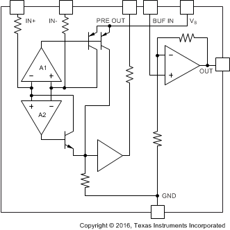
The INA27xA-Q1 is a family of voltage output current-sense amplifiers. INA27xA-Q1 operates over a wide common-mode voltage range (–16 V to +80 V). The package brings out the output of the pre amplifier stage (PRE OUT) and the input to the output buffer stage (BUF IN). This pinout readily enables filtering, see First- or Second-Order Filtering.

Functional Block Diagram

INA270A-Q1 INA271A-Q1 fbd_sbos401.gif

Feature Description

Output Voltage Range

The output of the INA27xA-Q1 is accurate within the output voltage swing range set by the power-supply pin, VS.

Device Functional Modes

First- or Second-Order Filtering

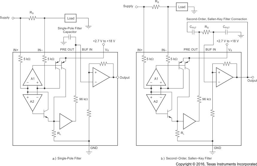
The INA27xA-Q1 devices readily enable the inclusion of filtering between the preamp output and buffer input. Single-pole filtering can be accomplished with a single capacitor because of the 96-kΩ output impedance at PRE OUT on pin 3 (see Figure 15a).

The INA27xA-Q1 devices readily lend themselves to second-order Sallen-Key configurations (see Figure 15b). When designing these configurations consider that the PRE OUT 96-kΩ output impedance exhibits an initial variation of ±30% with the addition of a –2200-ppm/°C temperature coefficient.
INA270A-Q1 INA271A-Q1 ai_easy_filter.gif
The INA27xA-Q1 can be easily connected for first-order or second-order filtering. Remember to use the appropriate buffer gain (INA270A-Q1 = 1.4, INA271A-Q1 = 2) when designing Sallen-Key configurations.
Figure 15. First-Order or Second-Order Filtering