ZHCSHF9E February   2007  – January 2018 INA270 , INA271

PRODUCTION DATA.  

  1. 特性
  2. 应用
  3. 说明
    1.     Device Images
      1.      简化原理图
  4. 修订历史记录
  5. Device Comparison Table
  6. Pin Configuration and Functions
    1.     Pin Functions
  7. Specifications
    1. 7.1 Absolute Maximum Ratings
    2. 7.2 ESD Ratings
    3. 7.3 Recommended Operating Conditions
    4. 7.4 Thermal Information
    5. 7.5 Electrical Characteristics
    6. 7.6 Typical Characteristics
  8. Detailed Description
    1. 8.1 Overview
    2. 8.2 Functional Block Diagram
    3. 8.3 Feature Description
      1. 8.3.1 Basic Connection
      2. 8.3.2 Selecting RS
      3. 8.3.3 Transient Protection
    4. 8.4 Device Functional Modes
      1. 8.4.1 First- or Second-Order Filtering
      2. 8.4.2 Accuracy Variations as a Result of VSENSE and Common-Mode Voltage
        1. 8.4.2.1 Normal Case 1: VSENSE ≥ 20 mV, VCM ≥ VS
        2. 8.4.2.2 Normal Case 2: VSENSE ≥ 20 mV, VCM < VS
        3. 8.4.2.3 Low VSENSE Case 1: VSENSE < 20 mV, –16 V ≤ VCM < 0; and Low VSENSE Case 3: VSENSE < 20 mV, VS < VCM ≤ 80 V
        4. 8.4.2.4 Low VSENSE Case 2: VSENSE < 20 mV, 0 V ≤ VCM ≤ VS
  9. Application and Implementation
    1. 9.1 Application Information
    2. 9.2 Typical Application
      1. 9.2.1 Design Requirements
      2. 9.2.2 Detailed Design Procedure
      3. 9.2.3 Application Curves
  10. 10Power Supply Recommendations
    1. 10.1 Shutdown
  11. 11Layout
    1. 11.1 Layout Guidelines
      1. 11.1.1 RFI and EMI
    2. 11.2 Layout Example
  12. 12器件和文档支持
    1. 12.1 Documentation Support
      1. 12.1.1 相关文档
    2. 12.2 相关链接
    3. 12.3 社区资源
    4. 12.4 商标
    5. 12.5 静电放电警告
    6. 12.6 Glossary
  13. 13机械、封装和可订购信息

封装选项

机械数据 (封装 | 引脚)
散热焊盘机械数据 (封装 | 引脚)
订购信息

Low VSENSE Case 2: VSENSE< 20 mV, 0 V ≤ VCM ≤ VS

This region of operation is the least accurate for the INA270 family. To achieve the wide input common-mode voltage range, these devices use two op amp front ends in parallel. One op amp front end operates in the positive input common-mode voltage range, and the other in the negative input region. For this case, neither of these two internal amplifiers dominates and overall loop gain is very low. Within this region, VOUT approaches voltages close to linear operation levels for Normal Case 2.

This deviation from linear operation becomes greatest the closer VSENSE approaches 0 V. Within this region, when VSENSE approaches 20 mV, device operation is closer to that described by Normal Case 2. Figure 18 shows this behavior for the INA271. The VOUT maximum peak for this case is determined by maintaining a constant VS, setting VSENSE = 0 mV, and sweeping VCM from 0 V to VS. The exact VCM at which VOUT peaks during this case varies from device to device. The maximum peak voltage for the INA270 is 0.28 V; for the INA271, the maximum peak voltage is 0.4 V.
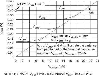
INA270 INA271 ai_exam_case2_bos381.gif
Figure 18. Example for Low VSENSE Case 2 (INA271, Gain = 20)