ZHCS078B June 2011 – September 2024 INA226
PRODUCTION DATA
- 1
- 1 特性
- 2 应用
- 3 说明
- 4 Pin Configuration and Functions
- 5 Specifications
-
6 Detailed Description
- 6.1 Overview
- 6.2 Functional Block Diagram
- 6.3 Feature Description
- 6.4 Device Functional Modes
- 6.5 Programming
- 7 Registers
- 8 Application and Implementation
- 9 Device and Documentation Support
- 10Revision History
- 11Mechanical, Packaging, and Orderable Information
4 Pin Configuration and Functions
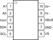
 Figure 4-1 DGS Package10-Pin VSSOPTop View
Table 4-1 Pin Functions
| PIN | Type | DESCRIPTION | |
|---|---|---|---|
| NAME | NO. | ||
| A0 | 2 | Digital input | Address pin. Connect to GND, SCL, SDA, or VS. Table 6-2 shows pin settings and corresponding addresses. |
| A1 | 1 | Digital input | Address pin. Connect to GND, SCL, SDA, or VS. Table 6-2 shows pin settings and corresponding addresses. |
| Alert | 3 | Digital output | Multi-functional alert, open-drain output. |
| GND | 7 | Analog | Ground. |
| IN+ | 10 | Analog input | Connect to supply side of shunt resistor. |
| IN– | 9 | Analog input | Connect to load side of shunt resistor. |
| SCL | 5 | Digital input | Serial bus clock line, open-drain input. |
| SDA | 4 | Digital I/O | Serial bus data line, open-drain input/output. |
| VBUS | 8 | Analog input | Bus voltage input. |
| VS | 6 | Analog | Power supply, 2.7 V to 5.5 V. |