at TA = 25 °C, VS = 1.8 V, VIN+ = 12 V, VENABLE = VS, VREF = GND and all gain options (unless otherwise noted)
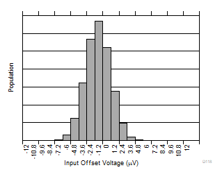 Figure 6-1 Input Offset Voltage Production Distribution
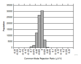 Figure 6-3 Common-Mode Rejection Production Distribution
 Figure 6-5 Gain Error Production Distribution (INA191)
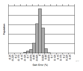 Figure 6-7 Gain Error Production Distribution
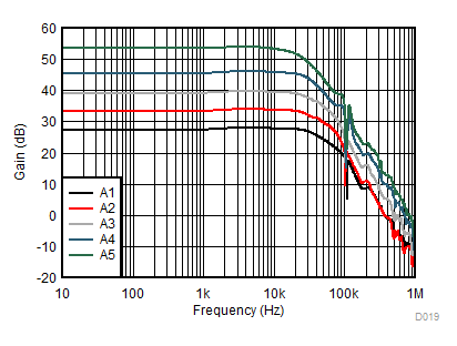 Figure 6-9 Gain vs. Frequency
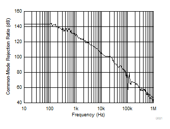 Figure 6-11 Common-Mode Rejection Ratio vs. Frequency
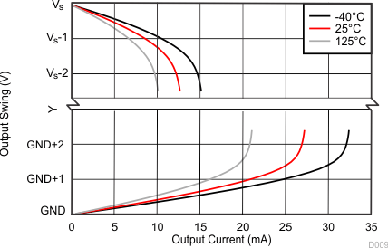 Figure 6-13 Output Voltage Swing vs. Output Current
| VENABLE = 0 V, VSENSE = 0 V |
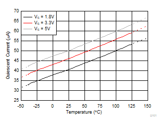 Figure 6-17 Quiescent Current vs. Temperature (INA191)
| VENABLE1 = VENABLE2 =
VS ,
VREF = VS /2 |
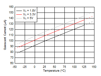
Figure 6-19 Quiescent Current vs. Temperature (INA2191 )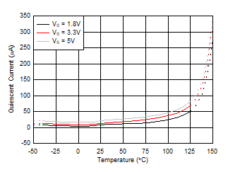
| VENABLE1 = VENABLE2 = 0 V,
VREF = VS /2 |
Figure 6-21 Quiescent Current vs. Temperature (INA2191 Disabled)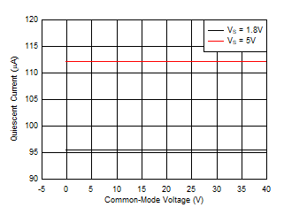 Figure 6-23 Quiescent Current vs. Common-Mode Voltage (INA2191)
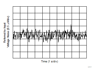 Figure 6-25 0.1-Hz to 10-Hz Input-Referred Voltage Noise
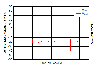 Figure 6-27 Common-Mode Voltage Transient Response
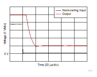 Figure 6-29 Noninverting Differential Input Overload Recovery
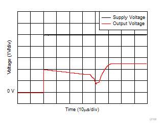
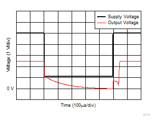 Figure 6-31 Brownout Recovery
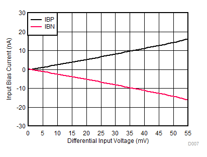
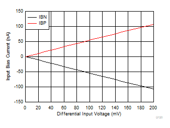 Figure 6-33 IB+ and IB– vs. Differential Input Voltage (INA191)
| VS = 5.0 V, VREF = VS /2, A1 device |
| VS = 5.0 V, VENABLE = 0 V, A1, A2, A3 devices |
| VS = 5.0 V, VENABLE = 0 V,
VREF = 2.5 V, A1, A2, A3 devices |
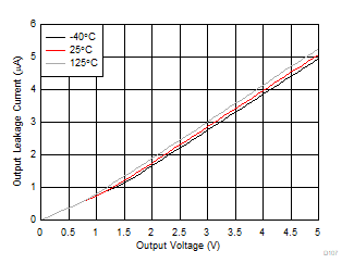
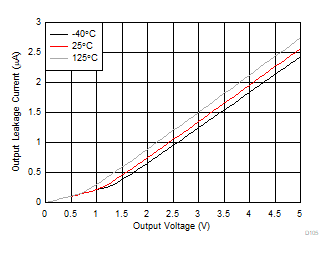
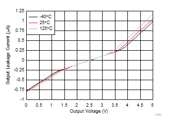
Figure 6-39 Output Leakage vs. Output Voltage (INA2191)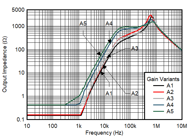 Figure 6-41 Output Impedance vs. Frequency
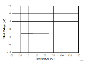 Figure 6-2 Offset Voltage vs. Temperature
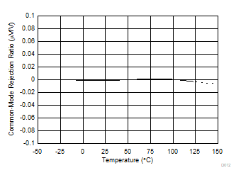 Figure 6-4 Common-Mode Rejection Ratio vs. Temperature
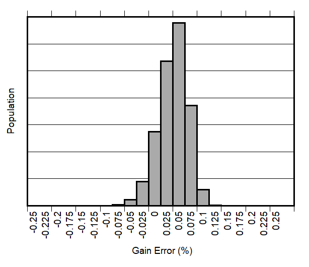 Figure 6-6 Gain
Error Production Distribution (INA2191)
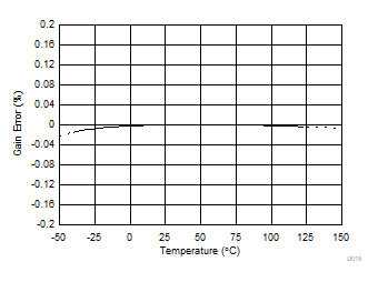 Figure 6-8 Gain Error vs. Temperature
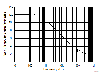 Figure 6-10 Power-Supply Rejection Ratio vs. Frequency
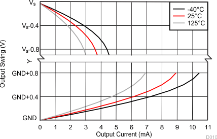 Figure 6-12 Output Voltage Swing vs. Output Current
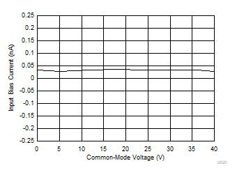
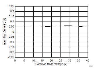 Figure 6-14 Input Bias Current vs. Common-Mode Voltage
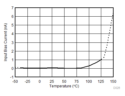 Figure 6-16 Input Bias Current vs. Temperature
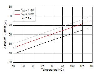
| Single channel enabled, VREF = VS
/2 |
Figure 6-18 Quiescent Current vs. Temperature (INA2191 )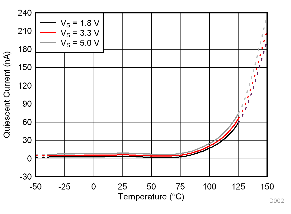 Figure 6-20 Quiescent Current vs. Temperature (INA191 Disabled)
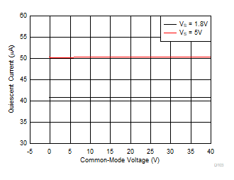 Figure 6-22 Quiescent Current vs. Common-Mode Voltage (INA191)
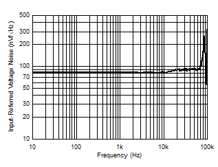 Figure 6-24 Input-Referred Voltage Noise vs. Frequency
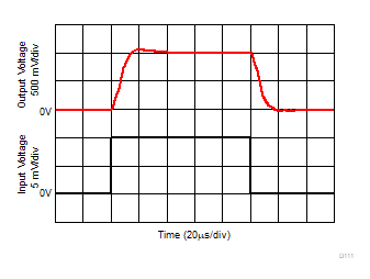
| VS = 5.0 V, 10-mVPP input step |
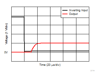 Figure 6-28 Inverting Differential Input Overload Recovery
 Figure 6-30 Start-Up Response
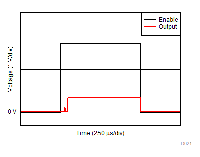
 Figure 6-32 Enable and Disable Response
| VS = 5.0 V, A2, A3, A4, A5 devices |

| VS = 5.0 V, VREF =
VS /2, A2, A3, A4, A5 devices |
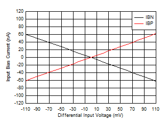
Figure 6-36 IB+
and IB– vs. Differential Input Voltage (INA2191)
| VS = 5.0 V, VENABLE = 0 V, A4, A5 devices |

| VS = 5.0 V, VENABLE = 0 V,
VREF = 2.5 V, A4, A5 devices |
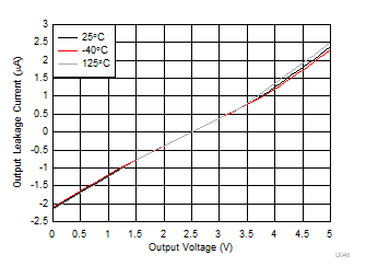
Figure 6-40 Output Leakage vs. Output Voltage (INA2191)
| VS = 5.0 V, VCM = 0 V,
VREF = VS /2 |
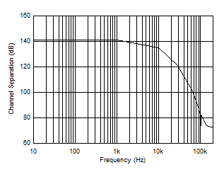
Figure 6-42 Channel Separation vs. Frequency (INA2191)


 Figure 6-11 Common-Mode Rejection Ratio vs. Frequency


 Figure 6-27 Common-Mode Voltage Transient Response


 Figure 6-8 Gain Error vs. Temperature


 Figure 6-22 Quiescent Current vs. Common-Mode Voltage (INA191)

 Figure 6-28 Inverting Differential Input Overload Recovery