SBOS360F June 2006 – November 2015 INA206 , INA207 , INA208
PRODUCTION DATA.
- 1 Features
- 2 Applications
- 3 Description
- 4 Revision History
- 5 Device Comparison Table
- 6 Pin Configuration and Functions
-
7 Specifications
- 7.1 Absolute Maximum Ratings
- 7.2 ESD Ratings
- 7.3 Recommended Operating Conditions
- 7.4 Thermal Information
- 7.5 Electrical Characteristics: Current-Shunt Monitor
- 7.6 Electrical Characteristics: Comparator
- 7.7 Electrical Characteristics: Reference
- 7.8 Electrical Characteristics: General
- 7.9 Typical Characteristics
- 8 Detailed Description
- 9 Application and Implementation
- 10Power Supply Recommendations
- 11Layout
- 12Device and Documentation Support
- 13Mechanical, Packaging, and Orderable Information
封装选项
请参考 PDF 数据表获取器件具体的封装图。
机械数据 (封装 | 引脚)
- D|14
- DGS|10
- PW|14
散热焊盘机械数据 (封装 | 引脚)
订购信息
8 Detailed Description
8.1 Overview
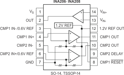
The INA206, INA207, and INA208 are a family of unidirectional current-shunt monitors with voltage output, dual comparators, and voltage reference. The INA206, INA207, and INA208 can sense drops across shunts at common-mode voltages from –16 V to 80 V. The INA206, INA207, and INA208 are available with three output voltage scales: 20 V/V, 50 V/V, and 100 V/V, with up to 500-kHz bandwidth. The INA206, INA207, and INA208 also incorporate two open-drain comparators with internal 0.6-V references. On 14-pin versions, the comparator references can be overridden by external inputs. Comparator 1 includes a latching capability, and Comparator 2 has a user-programmable delay. 14-pin versions also provide a 1.2-V reference output. The INA206, INA207, and INA208 operate from a single 2.7-V to 18-V supply. They are specified over the extended operating temperature range of –40°C to 125°C
8.2 Functional Block Diagram
8.3 Feature Description
8.3.1 Output Voltage Range
The output of the INA206, INA207, and INA208 is accurate within the output voltage swing range set by the power supply pin, Vs. This performance is best illustrated when using the INA208 (a gain of 100 version), where a 100-mV full-scale input from the shunt resistor requires an output voltage swing of 10 V, and a power-supply voltage sufficient to achieve 10 V on the output.
8.3.2 Reference
The INA206, INA207, and INA208 include an internal voltage reference that has a load regulation of 0.4 mV/mA (typical), and not more than 100 ppm/°C of drift. Only the 14-pin package allows external access to reference voltages, where voltages of 1.2 V and 0.6 V are both available. Output current versus output voltage is illustrated in Typical Characteristics.
8.3.3 Comparator
The INA206, INA207, and INA208 devices incorporate two open-drain comparators. These comparators typically have 2 mV of offset and a 1.3-µs (typical) response time. The output of Comparator 1 latches and is reset through the CMP1 RESET pin, as shown in Figure 31. This configuration applies to both the 10- and 14-pin versions. Figure 30 illustrates the comparator delay.
The 14-pin versions of the INA206, INA207, and INA208 include additional features for comparator functions. The comparator reference voltage of both Comparator 1 and Comparator 2 can be overridden by external inputs for increased design flexibility. Comparator 2 has a programmable delay.
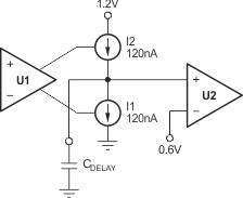 Figure 30. Simplified Model of the Comparator 2 Delay Circuit
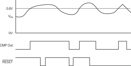 Figure 31. Comparator 1 Latching Capability
8.3.4 Comparator Delay (14-Pin Version Only)
The Comparator 2 programmable delay is controlled by a capacitor connected to the CMP2 Delay Pin; see Figure 40. The capacitor value (in µF) is selected by using Equation 1.

A simplified version of the delay circuit for Comparator 2 is shown in Figure 30. The delay comparator consists of two comparator stages with the delay between them. Note that I1 and I2 cannot be turned on simultaneously; I1 corresponds to a U1 low output and I2 corresponds to a U1 high output. Using an initial assumption that the U1 output is low, I1 is on, then U2 +IN is zero. If U1 goes high, I2 supplies 120 nA to CDELAY. The voltage at U2 +IN begins to ramp toward a 0.6-V threshold. When the voltage crosses this threshold, the U2 output goes high while the voltage at U2 +IN continues to ramp up to a maximum of 1.2 V when given sufficient time (twice the value of the delay specified for CDELAY). This entire sequence is reversed when the comparator outputs go low, so that returning to low exhibits the same delay.
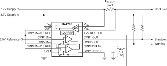 Figure 32. Server 12-V Supply Current Monitor
It is important to note what will happen if events occur more rapidly than the delay timeout; for example, when the U1 output goes high (turning on I2), but returns low (turning I1 back on) prior to reaching the 0.6-V transition for U2. The voltage at U2 +IN ramps back down at a rate determined by the value of CDELAY, and only returns to zero if given sufficient time.
In essence, when analyzing Comparator 2 for behavior with events more rapid than its delay setting, use the model shown in Figure 30.
8.3.5 Comparator Maximum Input Voltage Range
The maximum voltage at the comparator input for normal operation is up to (Vs) – 1.5 V. There are special considerations when overdriving the reference inputs (pins 3 and 6). Driving either or both inputs high enough to drive 1 mA back into the reference introduces errors into the reference. Figure 33 shows the basic input structure. A general guideline is to limit the voltage on both inputs to a total of 20 V. The exact limit depends on the available voltage and whether either or both inputs are subject to the large voltage. When making this determination, consider the 20 kΩ from each input back to the comparator. Figure 34 shows the maximum input voltage that avoids creating a reference error when driving both inputs (an equivalent resistance back into the reference of 10 kΩ.
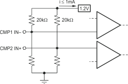 Figure 33. Limit Current Into Reference ≤ 1 mA
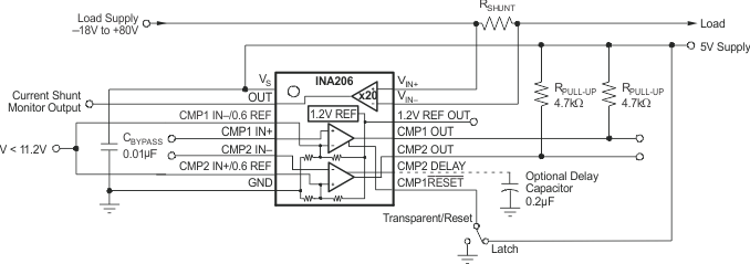 Figure 34. Overdriving Comparator Inputs Without Generating a Reference Error
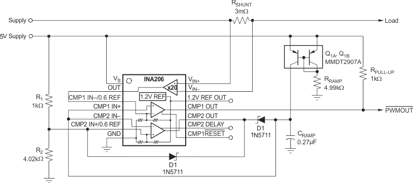 Figure 35. PWM Output Current-Shunt Monitor
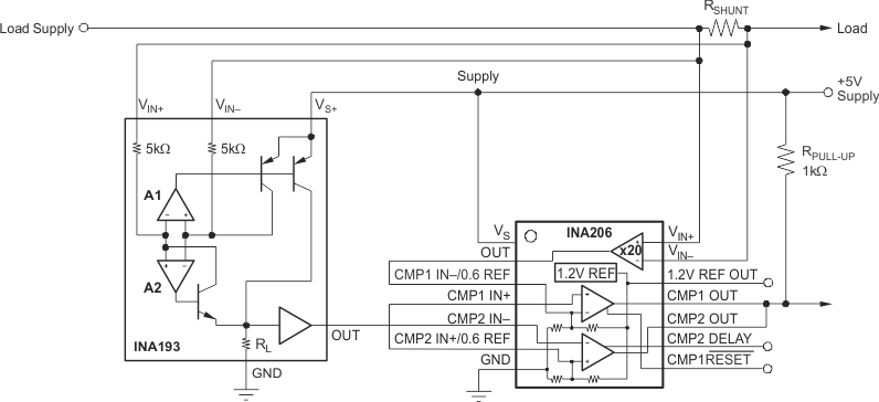 Figure 36. Bi-Directional Current Comparator
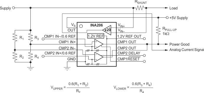 Figure 37. Analog Output Current-Shunt Monitor With Comparators Used as Power-Supply Under-Limit or Over-Limit or Power-Good Detector
8.4 Device Functional Modes
8.4.1 Accuracy Variations as a Result of VSENSE and Common-Mode Voltage
The accuracy of the INA206, INA207, and INA208 current-shunt monitors is a function of two main variables: VSENSE (VIN+ – VIN–) and common-mode voltage, VCM, relative to the supply voltage, VS. VCM is expressed as (VIN+ + VIN–)/2; however, in practice, VCM is seen as the voltage at VIN+ because the voltage drop across VSENSE is usually small.
This section addresses the accuracy of these specific operating regions:
- Normal Case 1: VSENSE ≥ 20 mV, VCM ≥ VS
- Normal Case 2: VSENSE ≥ 20 mV, VCM < VS
- Low VSENSE Case 1: VSENSE < 20 mV, –16 V ≤ VCM < 0
- Low VSENSE Case 2: VSENSE < 20 mV, 0 V ≤ VCM ≤ VS
- Low VSENSE Case 3: VSENSE < 20 mV, VS < VCM ≤ 80 V
8.4.1.1 Normal Case 1: VSENSE ≥ 20 mV, VCM ≥ VS
This region of operation provides the highest accuracy. Here, the input offset voltage is characterized and measured using a two-step method. First, the gain is determined by Equation 2.

where
- VOUT1 = Output Voltage with VSENSE = 100 mV
- VOUT2 = Output Voltage with VSENSE = 20 mV
Then the offset voltage is measured at VSENSE = 100 mV and referred to the input (RTI) of the current-shunt monitor, as shown in Equation 3

In the Typical Characteristics, the Output Error vs Common-Mode Voltage curve shows the highest accuracy for this region of operation. In this plot, VS = 12 V; for VCM ≥ 12 V, the output error is at its minimum. This case is also used to create the VSENSE ≥ 20-mV output specifications in Electrical Characteristics: Current-Shunt Monitor through Electrical Characteristics: General.
8.4.1.2 Normal Case 2: VSENSE ≥ 20 mV, VCM < VS
This region of operation has slightly less accuracy than Normal Case 1 as a result of the common-mode operating area in which the part functions, as seen in the Output Error vs Common-mode Voltage curve. As noted, for this graph VS = 12 V; for VCM < 12 V, the Output Error increases as VCM becomes less than 12 V, with a typical maximum error of 0.005% at the most negative VCM = –16 V.
| Low VSENSE Case 1: | VSENSE < 20 mV, –16 V ≤ VCM < 0; and |
| Low VSENSE Case 3: | VSENSE < 20 mV, VS < VCM ≤ 80 V |
Although the INA206 family of devices are not designed for accurate operation in either of these regions, some applications are exposed to these conditions; for example, when monitoring power supplies that are switched on and off while VS is still applied to the INA206, INA207, or INA208. It is important to know what the behavior of the devices will be in these regions.
As VSENSE approaches 0 mV, in these VCM regions, the device output accuracy degrades. A larger-than-normal offset can appear at the currenrt-shunt monitor output with a typical maximum value of VOUT = 300 mV for VSENSE = 0 mV. As VSENSE approaches 20 mV, VOUT Returns to the expected output value with accuracy as specified in Electrical Characteristics: Current-Shunt Monitor through Electrical Characteristics: General. Figure 38 illustrates this effect using the INA208 (Gain = 100).
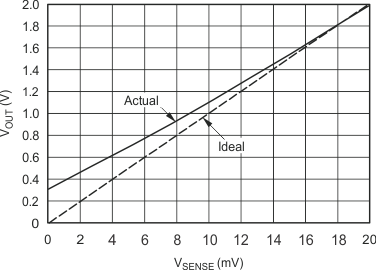 Figure 38. Example for Low VSENSE Cases 1 and 3 (INA208, Gain = 100)
8.4.1.3 Low VSENSE Case 2: VSENSE < 20mV, 0V ≤ VCM ≤ VS
This region of operation is the least accurate for the INA206 family. To achieve the wide input common-mode voltage range, these devices use two op amp front ends in parallel. One op amp front end operates in the positive input common-mode voltage range, and the other in the negative input region. For this case, neither of these two internal amplifiers dominates and overall loop gain is very low. Within this region, VOUT approaches voltages close to linear operation levels for Normal Case 2. This deviation from linear operation becomes greatest the closer VSENSE approaches 0 V. Within this region, as VSENSE approaches 20 mV, device operation is closer o that described by Normal Case 2. Figure 39 illustrates this behavior for the INA208. The VOUT maximum peak for this case is tested by maintaining a constant VS, setting VSENSE = 0 mV and sweeping VCM from 0 V to VS. The exact VCM at which VOUT peaks during this test varies from part to part, but the VOUT maximum peak is tested to be less than the specified VOUT Tested Limit.
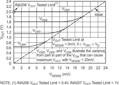 Figure 39. Example for Low VSENSE Case 2 (INA208, Gain = 100)