SBOS360F June 2006 – November 2015 INA206 , INA207 , INA208
PRODUCTION DATA.
- 1 Features
- 2 Applications
- 3 Description
- 4 Revision History
- 5 Device Comparison Table
- 6 Pin Configuration and Functions
-
7 Specifications
- 7.1 Absolute Maximum Ratings
- 7.2 ESD Ratings
- 7.3 Recommended Operating Conditions
- 7.4 Thermal Information
- 7.5 Electrical Characteristics: Current-Shunt Monitor
- 7.6 Electrical Characteristics: Comparator
- 7.7 Electrical Characteristics: Reference
- 7.8 Electrical Characteristics: General
- 7.9 Typical Characteristics
- 8 Detailed Description
- 9 Application and Implementation
- 10Power Supply Recommendations
- 11Layout
- 12Device and Documentation Support
- 13Mechanical, Packaging, and Orderable Information
封装选项
请参考 PDF 数据表获取器件具体的封装图。
机械数据 (封装 | 引脚)
- D|14
- DGS|10
- PW|14
散热焊盘机械数据 (封装 | 引脚)
订购信息
7 Specifications
7.1 Absolute Maximum Ratings
over operating free-air temperature range (unless otherwise noted) (1)| MIN | MAX | UNIT | ||
|---|---|---|---|---|
| Supply voltage, Vs | 18 | V | ||
| Current-shunt monitor analog inputs, VIN+ and VIN– |
Differential (VIN+) – (VIN–) | –18 | 18 | V |
| Common-Mode | –16 | 80 | V | |
| Comparator analog input and reset pins | GND – 0.3 | (Vs) + 0.3 | V | |
| Analog output, out pin | GND – 0.3 | (Vs) + 0.3 | V | |
| Comparator output, out pin | GND – 0.3 | 18 | V | |
| VREF and CMP2 delay pin | GND – 0.3 | 10 | V | |
| Input current into any pin | 5 | mA | ||
| Operating temperature | –55 | 150 | °C | |
| Junction temperature | –65 | 150 | °C | |
| Storage temperature, Tstg | –65 | 150 | °C | |
(1) Stresses beyond those listed under Absolute Maximum Ratings may cause permanent damage to the device. These are stress ratings only, which do not imply functional operation of the device at these or any other conditions beyond those indicated under Recommended Operating Conditions. Exposure to absolute-maximum-rated conditions for extended periods may affect device reliability.
7.2 ESD Ratings
| VALUE | UNIT | ||||
|---|---|---|---|---|---|
| V(ESD) | Electrostatic discharge | Human body model (HBM), per ANSI/ESDA/JEDEC JS-001(1) | ±4000 | V | |
| Charged device model (CDM), per JEDEC specification JESD22-C101(2) | ±500 | ||||
(1) JEDEC document JEP155 states that 500-V HBM allows safe manufacturing with a standard ESD control process.
(2) JEDEC document JEP157 states that 250-V CDM allows safe manufacturing with a standard ESD control process.
7.3 Recommended Operating Conditions
over operating free-air temperature range (unless otherwise noted)| MIN | NOM | MAX | UNIT | ||
|---|---|---|---|---|---|
| Vcm Common-mode input voltage | –16 | 12 | 80 | V | |
| Vs Operating supply voltage | 2.7 | 12 | 18 | V | |
| TA Operating free-air temperature | –40 | 25 | 125 | ºC | |
7.4 Thermal Information
| THERMAL METRIC (1) | INA20x | UNIT | |||
|---|---|---|---|---|---|
| D (SOIC) | DGS (VSSOP) | PW (TSSOP) | |||
| 14 PINS | 10 PINS | 14 PINS | |||
| RθJA | Junction-to-ambient thermal resistance | 84.9 | 161.3 | 112.6 | °C/W |
| RθJC(top) | Junction-to-case (top) thermal resistance | 44 | 36.8 | 37.2 | °C/W |
| RθJB | Junction-to-board thermal resistance | 39.4 | 82.3 | 55.4 | °C/W |
| ψJT | Junction-to-top characterization parameter | 10.3 | 1.3 | 2.7 | °C/W |
| ψJB | Junction-to-board characterization parameter | 39.1 | 80.8 | 54.7 | °C/W |
| RθJC(bot) | Junction-to-case (bottom) thermal resistance | 150 | 200 | 150 | °C/W |
(1) For more information about traditional and new thermal metrics, see the Semiconductor and IC Package Thermal Metrics application report, SPRA953.
7.5 Electrical Characteristics: Current-Shunt Monitor
At TA = 25°C, VS = 12 V, VIN+ = 12 V, VSENSE = 100 mV, RL = 10 kΩ to GND, RPULL-UP = 5.1 kΩ each connected from CMP1 OUT and CMP2 OUT to VS, and CMP1 IN+ = 1 V and CMP2 IN– = GND, unless otherwise noted.| PARAMETERS | TEST CONDITIONS | MIN | TYP | MAX | UNIT | |||
|---|---|---|---|---|---|---|---|---|
| INPUT | ||||||||
| VSENSE | Full-scale sense input voltage | VSENSE = VIN+ – VIN– | 0.15 | (VS –0.25)/Gain | V | |||
| VCM | Common-mode input range | TA = –40°C to 125°C | –16 | 80 | V | |||
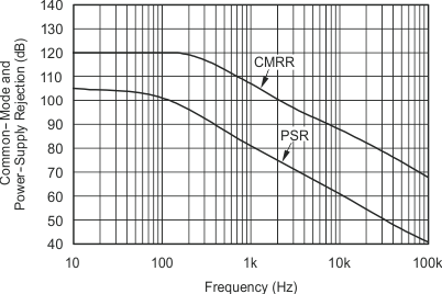
| CMRR | Common-mode rejection ratio | VIN+ = –16 V to 80 V | 80 | 100 | dB | |||
| Common-mode rejection ratio over temperature | VIN+ = 12 V to 80 V, TA = –40°C to 125°C | 100 | 123 | dB | ||||
| VOS | Offset voltage RTI (1) | TA = 25°C | ±0.5 | ±2.5 | mV | |||
| TA = 25°C to 125°C | ±3 | |||||||
| TA = –40°C to 25°C | ±3.5 | |||||||
| dVOS/dT | Offset voltage RTI vs temperature | TA = –40°C to 125°C | 5 | µV/°C | ||||
| PSR | Offset voltage RTI vs power supply | VOUT = 2 V, VIN+ = 18 V, 2.7 V, TA = –40°C to 125°C | 2.5 | 100 | µV/V | |||
| IB | Input bias current, VIN– Pin | TA = –40°C to 125°C | ±9 | ±16 | µA | |||
| OUTPUT (VSENSE ≥ 20 mV) | ||||||||
| G | Gain | INA206 | 20 | V/V | ||||
| INA207 | 50 | |||||||
| INA208 | 100 | |||||||
| Gain error | VSENSE = 20 mV to 100 mV | ±0.2% | ±1% | |||||
| Gain error over temperature | VSENSE = 20 mV to 100 mV, TA = –40°C to 125°C | ±2% | ||||||
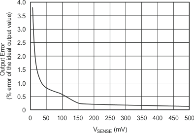
| Total output error (2) | VSENSE = 120 mV, VS = 16 V | ±0.75% | ±2.2% | |||||
| Total output error over temperature | VSENSE = 120 mV, VS = 16 V, TA = –40°C to 125°C | ±3.5% | ||||||
| Nonlinearity error (3) | VSENSE = 20 mV to 100 mV | ±0.002% | ||||||
| RO | Output impedance | 1.5 | Ω | |||||
| Maximum capacitive load | No Sustained Oscillation | 10 | nF | |||||
| OUTPUT (VSENSE < 20 mV) (4) | ||||||||
| Output voltage | INA206 | –16 V ≤ VCM < 0 V | 300 | mV | ||||
| INA207 | 300 | |||||||
| INA208 | 300 | |||||||
| INA206 | 0 V ≤ VCM ≤ VS, VS = 5 V | 0.4 | V | |||||
| INA207 | 1 | |||||||
| INA208 | 2 | |||||||
| INA206 | VS < VCM ≤ 80 V | 300 | mV | |||||
| INA207 | 300 | |||||||
| INA208 | 300 | |||||||
| VOLTAGE OUTPUT | ||||||||
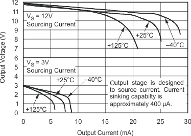
| Output swing to the positive rail | VIN– = 11 V, VIN+ = 12 V, TA = –40°C to 125°C | (Vs) – 0.15 | (Vs) – 0.25 | V | ||||
| Output swing to GND (5) | VIN– = 0 V, VIN+ = –0.5 V, TA = –40°C to 125°C | (VGND) + 0.004 | (VGND) + 0.05 | V | ||||
| FREQUENCY RESPONSE | ||||||||
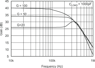
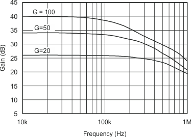
| Bandwidth | INA206 | CLOAD = 5 pF | 500 | kHz | ||||
| INA207 | 300 | |||||||
| INA208 | 200 | |||||||
| Phase margin | CLOAD < 10 pF | 40 | ° | |||||
| Slew rate | 1 | V/µs | ||||||
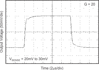
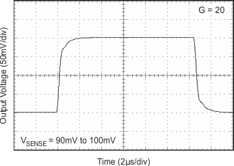
| Settling time (1%) | VSENSE = 10 mVPP to 100 mVPP, CLOAD = 5 pF | 2 | µs | |||||
| NOISE, RTI | ||||||||
| Output voltage noise density | 40 | nV/√Hz | ||||||
(1) Offset is extrapolated from measurements of the output at 20 mV and 100 mV VSENSE.
(2) Total output error includes effects of gain error and VOS.
(3) Linearity is best fit to a straight line.
(4) For details on this region of operation, see the Accuracy Variations as a Result of VSENSE and Common-Mode Voltage section.
(5) Specified by design.
7.6 Electrical Characteristics: Comparator
At TA = 25°C, VS = 12 V, VIN+ = 12 V, VSENSE = 100 mV, RL = 10 kΩ to GND, RPULL-UP = 5.1 kΩ each connected from CMP1 OUT and CMP2 OUT to VS, unless otherwise noted.| PARAMETERS | TEST CONDITIONS | MIN | TYP | MAX | UNIT | ||
|---|---|---|---|---|---|---|---|
| OFFSET VOLTAGE | |||||||
| Offset Voltage | Comparator Common-Mode Voltage = Threshold Voltage, Figure 1 | 2 | mV | ||||
| Offset Voltage Drift, Comparator 1 | TA = –40°C to 125°C | ±2 | µV/°C | ||||
| Offset Voltage Drift, Comparator 2 | TA = –40°C to 125°C | 5.4 | µV/°C | ||||
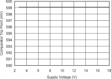
| Threshold | TA = 25°C | 590 | 608 | 620 | mV | ||
| Threshold over Temperature | TA = –40°C to 125°C | 586 | 625 | mV | |||
| Hysteresis (1), CMP1 | TA = –40°C to 85C | –8 | mV | ||||
| Hysteresis (1), CMP2 | TA = –40°C to 85°C | 8 | mV | ||||
| INPUT BIAS CURRENT (2) | |||||||
| CMP1 IN+, CMP2 IN– | 0.005 | 10 | nA | ||||
| CMP1 IN+, CMP2 IN– vs Temperature | TA = –40°C to 125°C | 15 | nA | ||||
| INPUT IMPEDANCE | |||||||
| Pins 3 and 6 (14-pin packages only) | 10 | kΩ | |||||
| INPUT RANGE | |||||||
| CMP1 IN+ and CMP2 IN– | 0 V to VS – 1.5V | V | |||||
| Pins 3 and 6 (14-pin packages only) (3) | 0 V to VS – 1.5V | V | |||||
| OUTPUT | |||||||
| Large-signal differential voltage gain | CMP VOUT 1 V to 4 V, RL ≥ 15 kΩ connected to 5 V | 200 | V/mV | ||||
| High-level output current | VID = 0.4 V, VOH = VS | 0.0001 | 1 | µA | |||
| Low-level output voltage | VID = –0.6 V, IOL = 2.35 mA | 220 | 300 | mV | |||
| RESPONSE TIME (3) | |||||||
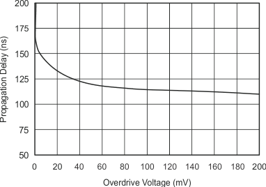
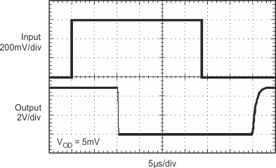
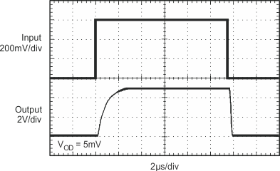
| Comparator 1 | RL to 5 V, CL = 15 pF, 100-mV Input Step with 5-mV Overdrive | 1.3 | µs | ||||
| Comparator 2 | RL to 5 V, CL = 15 pF, 100-mV Input Step with 5-mV Overdrive, CDELAY Pin Open | 1.3 | µs | ||||
| RESET | |||||||
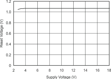
| RESET Threshold (4) | 1.1 | V | |||||
| Logic Input Impedance | 2 | mΩ | |||||
| Minimum RESET Pulse Width | 1.5 | µs | |||||
| RESET Propagation Delay | 3 | µs | |||||
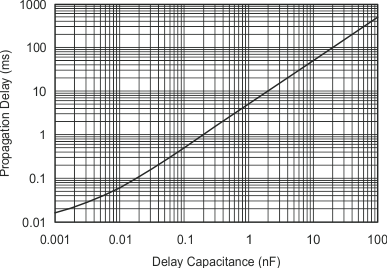
| Comparator 2 Delay Equation (5) | CDELAY = tD/5 | µF | |||||
| Comparator 2 Delay, tD | CDELAY = 0.1 μF | 0.5 | s | ||||
(1) Hysteresis refers to the threshold (the threshold specification applies to a rising edge of a noninverting input) of a falling edge on the noninverting input of the comparator. See Figure 1.
(2) Specified by design.
(3) The comparator response time specified is the interval between the input step function and the instant when the output crosses 1.4 V.
(4) RESET input has an internal 2 MΩ (typical) pull-down. Leaving RESET open results in a LOW state, with transparent comparator operation.
(5) The Comparator 2 delay applies to both rising and falling edges of the comparator output.
7.7 Electrical Characteristics: Reference
At TA = 25°C, VS = 12 V, VIN+ = 12 V, VSENSE = 100 mV, RL = 10 kΩ to GND, RPULL-UP = 5.1 kΩ each connected from CMP1 OUT and CMP2 OUT to VS, unless otherwise noted.| PARAMETERS | TEST CONDITIONS | MIN | TYP | MAX | UNIT | |||
|---|---|---|---|---|---|---|---|---|
| REFERENCE VOLTAGE | ||||||||
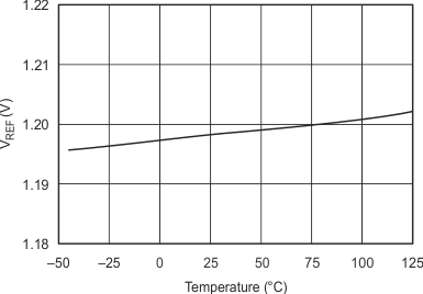
| 1.2VREFOUT Output Voltage | 1.188 | 1.2 | 1.212 | V | ||||
| dVOUT/dT | Reference Drift | TA = –40°C to 85°C | 40 | 100 | ppm/°C | |||
| 0.6VREF Output Voltage (Pins 3 and 6 of 14-pin packages only) |
0.6 | V | ||||||
| dVOUT/dT | Reference Drift | TA = –40°C to 85°C | 40 | 100 | ppm/°C | |||
| dVOUT/dILOAD | LOAD REGULATION | |||||||
| Sourcing | 0 mA < ISOURCE < 0.5 mA | 0.4 | 2 | mV/mA | ||||
| Sinking | 0 mA < ISINK < 0.5 mA | 0.4 | mV/mA | |||||
| ILOAD | LOAD CURRENT | TA = –40°C to 125°C | 1 | mA | ||||
| dVOUT/dVS | LINE REGULATION | 2.7 V < VS < 18 V, TA = –40°C to 125°C | 30 | µV/V | ||||
| CAPACITIVE LOAD | ||||||||
| Reference Output Maximum Capacitive Load | No Sustained Oscillations | 10 | nF | |||||
| OUTPUT IMPEDANCE | ||||||||
| Pins 3 and 6 of 14-Pin Packages Only | 10 | kΩ | ||||||
7.8 Electrical Characteristics: General
At TA = 25°C, VS = 12 V, VIN+ = 12 V, VSENSE = 100 mV, RL = 10 kΩ to GND, RPULL-UP = 5.1 kΩ each connected from CMP1 OUT and CMP2 OUT to VS, and CMP1 IN+ = 1 V and CMP2 IN– = GND, unless otherwise noted.| PARAMETERS | TEST CONDITIONS | MIN | TYP | MAX | UNIT | |||
|---|---|---|---|---|---|---|---|---|
| POWER SUPPLY | ||||||||
| VS | Operating Power Supply | TA = –40°C to 125°C | 2.7 | 18 | V | |||
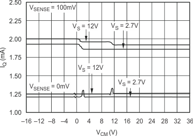
| IQ | Quiescent Current | VOUT = 2 V | 1.8 | 2.2 | mA | |||
| Quiescent Current over Temperature | VSENSE = 0 mV, TA = –40°C to 125°C | 2.8 | mA | |||||
| Comparator Power-On Reset Threshold (1) | 1.5 | V | ||||||
| TEMPERATURE | ||||||||
| Specified Temperature Range | –40 | 125 | °C | |||||
| Operating Temperature Range | –55 | 150 | °C | |||||
| Storage Temperature Range | –65 | 150 | °C | |||||
| θJA | Thermal Resistance | MSOP-10 Surface-Mount | 200 | °C/W | ||||
| SO-14, TSSOP-14 Surface-Mount | 150 | °C/W | ||||||
(1) The INA206, INA207, and INA208 are designed to power-up with the comparator in a defined reset state as long as CMP1 RESET is open or grounded. The comparator will be in reset as long as the power supply is below the voltage shown here. The comparator will assume a state based on the comparator input above this supply voltage. If CMP1 RESET is high at power-up, the comparator output comes up high and requires a reset to assume a low state, if appropriate.
 Figure 1. Comparator Hysteresis
7.9 Typical Characteristics
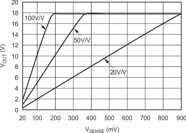
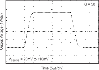
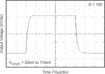
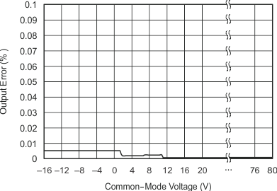
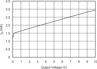
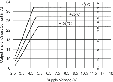
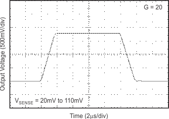
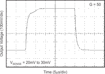
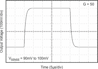
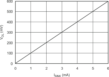
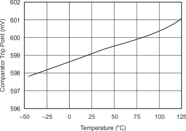
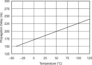
All specifications at TA = 25°C, VS = 12 V, VIN+ = 12 V, and VSENSE = 100 mV, unless otherwise noted.