ZHCSFN6F March 2007 – June 2021 INA203 , INA204 , INA205
PRODUCTION DATA
- 1 特性
- 2 应用
- 3 说明
- 4 Revision History
- 5 Pin Configuration and Functions
-
6 Specifications
- 6.1 Absolute Maximum Ratings
- 6.2 ESD Ratings
- 6.3 Recommended Operating Conditions
- 6.4 Thermal Information
- 6.5 Electrical Characteristics: Current-Shunt Monitor
- 6.6 Electrical Characteristics: Comparator
- 6.7 Electrical Characteristics: Reference
- 6.8 Electrical Characteristics: General
- 6.9 Typical Characteristics
- 7 Detailed Description
- 8 Application and Implementation
- 9 Power Supply Recommendations
- 10Layout
- 11Device and Documentation Support
- 12Mechanical, Packaging, and Orderable Information
封装选项
请参考 PDF 数据表获取器件具体的封装图。
机械数据 (封装 | 引脚)
- D|14
- DGS|10
- PW|14
散热焊盘机械数据 (封装 | 引脚)
订购信息
7.4.1 Input Filtering
An obvious and straightforward location for filtering is at the output of the INA203, INA204, and INA205 series; however, this location negates the advantage of the low output impedance of the internal buffer. The only other option for filtering is at the input pins of the INA203, INA204, and INA205, which is complicated by the internal 5 kΩ + 30% input impedance; this configuration is illustrated in Figure 7-10. Using the lowest possible resistor values minimizes both the initial shift in gain and effects of tolerance. Use Equation 2 to calculate the effect on initial gain.
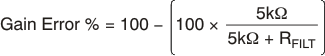
Total effect on gain error can be calculated by replacing the 5-kΩ term with 5 kΩ – 30%, (or 3.5 kΩ) or 5 kΩ + 30% (or 6.5 kΩ). The tolerance extremes of RFILT can also be inserted into the equation. If a pair of 100 Ω 1% resistors are used on the inputs, the initial gain error will be 1.96%. Worst-case tolerance conditions will always occur at the lower excursion of the internal 5-kΩ resistor (3.5 kΩ), and the higher excursion of RFILT – 3% in this case.
") Figure 7-10 Input Filter (Gain Error: 1.5% to –2.2%)
Figure 7-10 Input Filter (Gain Error: 1.5% to –2.2%)The specified accuracy of the INA203, INA204, and INA205 must then be combined in addition to these tolerances. While this discussion treated accuracy worst-case conditions by combining the extremes of the resistor values, it is appropriate to use geometric mean or root sum square calculations to total the effects of accuracy variations.