ZHCSFN4E November 2006 – September 2017 INA200 , INA201 , INA202
PRODUCTION DATA.
- 1 特性
- 2 应用
- 3 说明
- 4 修订历史记录
- 5 Pin Configuration and Functions
- 6 Specifications
- 7 Detailed Description
- 8 Application and Implementation
- 9 Power Supply Recommendations
- 10Layout
- 11器件和文档支持
- 12机械、封装和可订购信息
8 Application and Implementation
NOTE
Information in the following applications sections is not part of the TI component specification, and TI does not warrant its accuracy or completeness. TI’s customers are responsible for determining suitability of components for their purposes. Customers should validate and test their design implementation to confirm system functionality.
8.1 Application Information
The INA20x series is designed to enable simple configuration for detecting overcurrent conditions and current monitoring in an application. This device is individually targeted towards overcurrent detection of a single threshold. However, this device can pair with additional devices and circuitry to create more complex monitoring functional blocks.
8.2 Typical Application

8.2.1 Design Requirements
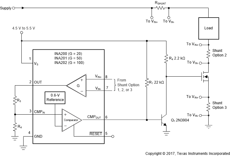
The device measures current through a resistive shunt with current flowing in one direction that enables detection of an overcurrent event only when the differential input voltage exceeds the threshold limit. When the current reaches the set limit of the divider R1 / R2, the output of CMPOUT transitions high, which turns Q1 on, pulls the gate of the pass-FET low, and turns off the flow off current.
8.2.2 Detailed Design Procedure
Figure 34 shows the basic connections of the device. The input terminals (IN+ and IN –) must be connected as closely as possible to the current-sensing resistor to minimize any resistance in series with the shunt resistance. Additional resistance between the current-sensing resistor and input terminals results in errors in the measurement. When input current flows through this external input resistance, the voltage developed across the shunt resistor differs from the voltage reaching the input terminals.
Use the gain of the INA20x and shunt value to calculate the OUT voltage for the desired trip current. Configure R1 and R2 so that the current trip point is equal to the 0.6-V reference voltage.
8.2.3 Application Curve
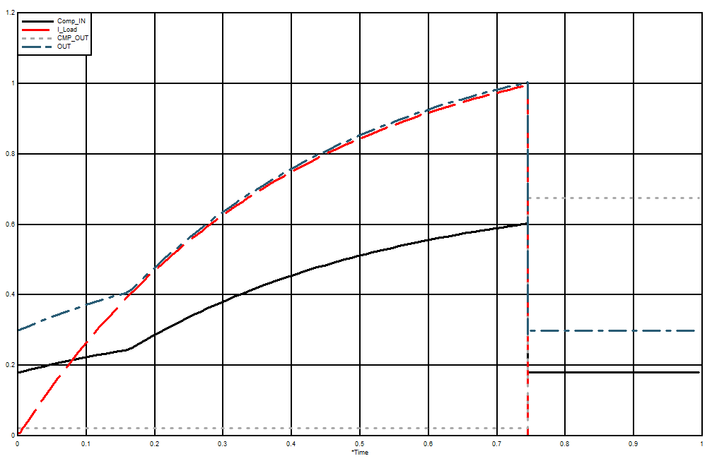
 Figure 35. Low-Side Switch Overcurrent Shutdown Response