ZHCSFN3E August   2006  – January 2021 INA193A-Q1 , INA194A-Q1 , INA195A-Q1 , INA196A-Q1 , INA197A-Q1 , INA198A-Q1

PRODUCTION DATA  

  1. 特性
  2. 应用
  3. 说明
  4. Revision History
  5. Pin Configuration and Functions
  6. Specifications
    1. 6.1 Absolute Maximum Ratings
    2. 6.2 ESD Ratings
    3. 6.3 Recommended Operating Conditions
    4. 6.4 Thermal Information
    5. 6.5 Electrical Characteristics
    6. 6.6 Typical Characteristics
  7. Detailed Description
    1. 7.1 Overview
    2. 7.2 Functional Block Diagram
    3. 7.3 Feature Description
      1. 7.3.1 Basic Connection
      2. 7.3.2 Selecting RS
      3. 7.3.3 Inside the INA19xA
      4. 7.3.4 Power Supply
    4. 7.4 Device Functional Modes
      1. 7.4.1 Input Filtering
      2. 7.4.2 Accuracy Variations as a Result Of VSENSE and Common Mode Voltage
        1. 7.4.2.1 Normal Case 1: VSENSE ≥ 20 mV, VCM ≥ VS
        2. 7.4.2.2 Normal Case 2: VSENSE ≥ 20 mV, VCM < VS
        3. 7.4.2.3 Low VSENSE Case 1: VSENSE < 20 mV, –16 V ≤ VCM < 0; and Low VSENSE Case 3: VSENSE < 20 mV, VS < VCM ≤ 80 V
        4. 7.4.2.4 Low VSENSE Case 2: VSENSE < 20 mV, 0 V ≤ VCM ≤ VS
      3. 7.4.3 Shutdown
      4. 7.4.4 Transient Protection
      5. 7.4.5 Output Voltage Range
  8. Application and Implementation
    1. 8.1 Application Information
    2. 8.2 Typical Application
      1. 8.2.1 Design Requirements
      2. 8.2.2 Detailed Design Procedure
      3. 8.2.3 Application Curve
  9. Power Supply Recommendations
  10. 10Layout
    1. 10.1 Layout Guidelines
      1. 10.1.1 RFI/EMI
    2. 10.2 Layout Example
  11. 11Device and Documentation Support
    1. 11.1 接收文档更新通知
    2. 11.2 支持资源
    3. 11.3 Trademarks
    4. 11.4 静电放电警告
    5. 11.5 术语表
  12. 12Mechanical, Packaging, and Orderable Information

封装选项

机械数据 (封装 | 引脚)
散热焊盘机械数据 (封装 | 引脚)
订购信息

Shutdown

Because the INA19xA-Q1 consume a quiescent current less than 1 mA, they can be powered by either the output of logic gates or by transistor switches to supply power. Use a totem pole output buffer or gate that can provide sufficient drive along with 0.1 μF bypass capacitor, preferably ceramic with good high frequency characteristics. This gate should have a supply voltage of 3 V or greater because the INA19xA-Q1 requires a minimum supply greater than 2.7 V. In addition to eliminating quiescent current, this gate also turns off the 10 μA bias current present at each of the inputs. An example shutdown circuit is shown in Figure 7-9.
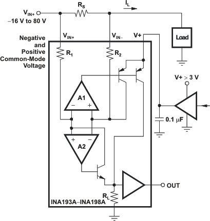
GUID-D1542E9C-AE14-4D72-833C-CB8345711B7C-low.gifFigure 7-9 INA19xA-Q1 Example Shutdown Circuit