ZHCSFN5E December   2000  – December 2015 INA139 , INA169

PRODUCTION DATA.  

  1. 特性
  2. 应用
  3. 说明
  4. 修订历史记录
  5. Pin Configuration and Functions
  6. Specifications
    1. 6.1 Absolute Maximum Ratings
    2. 6.2 ESD Ratings
    3. 6.3 Recommended Operating Conditions
    4. 6.4 Thermal Information
    5. 6.5 Electrical Characteristics
    6. 6.6 Typical Characteristics
  7. Detailed Description
    1. 7.1 Overview
    2. 7.2 Functional Block Diagram
    3. 7.3 Feature Description
      1. 7.3.1 Output Voltage Range
      2. 7.3.2 Bandwidth
    4. 7.4 Device Functional Modes
  8. Application and Implementation
    1. 8.1 Application Information
      1. 8.1.1 Operation
    2. 8.2 Typical Applications
      1. 8.2.1 Buffering Output to Drive an ADC
        1. 8.2.1.1 Design Requirements
        2. 8.2.1.2 Detailed Design Procedure
          1. 8.2.1.2.1 Selecting RS and RL
        3. 8.2.1.3 Application Curve
      2. 8.2.2 Output Filter
        1. 8.2.2.1 Design Requirements
        2. 8.2.2.2 Detailed Design Procedure
        3. 8.2.2.3 Application Curve
      3. 8.2.3 Offsetting the Output Voltage
      4. 8.2.4 Bipolar Current Measurement
        1. 8.2.4.1 Application Curve
      5. 8.2.5 Bipolar Current Measurement Using a Differential Input of the A/D Converter
      6. 8.2.6 Multiplexed Measurement Using Logic Signal for Power
  9. Power Supply Recommendations
  10. 10Layout
    1. 10.1 Layout Guidelines
    2. 10.2 Layout Example
  11. 11器件和文档支持
    1. 11.1 相关链接
    2. 11.2 社区资源
    3. 11.3 商标
    4. 11.4 静电放电警告
    5. 11.5 Glossary
  12. 12机械、封装和可订购信息

封装选项

请参考 PDF 数据表获取器件具体的封装图。

机械数据 (封装 | 引脚)
  • DBV|5
散热焊盘机械数据 (封装 | 引脚)
订购信息

Layout

Layout Guidelines

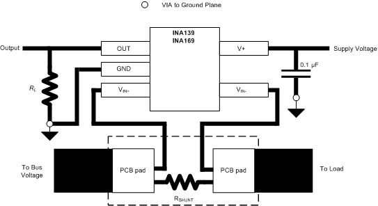
Figure 19 shows the basic connection of the INA139. The input pins, VIN+ and VIN–, must be connected as closely as possible to the shunt resistor to minimize any resistance in series with the shunt resistance. The output resistor, RL, is shown connected between pin 1 and ground. Best accuracy is achieved with the output voltage measured directly across RL. This is especially important in high-current systems where load current could flow in the ground connections, affecting the measurement accuracy.

No power-supply bypass capacitors are required for stability of the INA139. However, applications with noisy or high-impedance power supplies may require decoupling capacitors to reject power-supply noise; connect the bypass capacitors close to the device pins.

Layout Example

INA139 INA169 PCB_layout_sbos181.gif Figure 19. Typical Layout Example