SGLS185F September   2003  – May 2016 INA139-Q1 , INA169-Q1

PRODUCTION DATA.  

  1. Features
  2. Applications
  3. Description
  4. Revision History
  5. Pin Configuration and Functions
  6. Specifications
    1. 6.1 Absolute Maximum Ratings
    2. 6.2 ESD Ratings
    3. 6.3 Recommended Operating Conditions
    4. 6.4 Thermal Information
    5. 6.5 Electrical Characteristics
    6. 6.6 Typical Characteristics
  7. Detailed Description
    1. 7.1 Overview
    2. 7.2 Functional Block Diagram
    3. 7.3 Feature Description
      1. 7.3.1 Output Voltage Range
      2. 7.3.2 Bandwidth
    4. 7.4 Device Functional Modes
  8. Application and Implementation
    1. 8.1 Application Information
      1. 8.1.1 Operation
    2. 8.2 Typical Applications
      1. 8.2.1 Buffering Output to Drive an ADC
        1. 8.2.1.1 Design Requirements
        2. 8.2.1.2 Detailed Design Procedure
          1. 8.2.1.2.1 Selecting RS and RL
        3. 8.2.1.3 Application Curve
      2. 8.2.2 Output Filter
        1. 8.2.2.1 Design Requirements
        2. 8.2.2.2 Detailed Design Procedure
        3. 8.2.2.3 Application Curve
      3. 8.2.3 Offsetting the Output Voltage
      4. 8.2.4 Bipolar Current Measurement
        1. 8.2.4.1 Application Curve
      5. 8.2.5 Bipolar Current Measurement Using Differential Input of the ADC
      6. 8.2.6 Multiplexed Measurement Using Logic Signal for Power
  9. Power Supply Recommendations
  10. 10Layout
    1. 10.1 Layout Guidelines
    2. 10.2 Layout Example
  11. 11Device and Documentation Support
    1. 11.1 Related Documentation
    2. 11.2 Related Links
    3. 11.3 Community Resources
    4. 11.4 Trademarks
    5. 11.5 Electrostatic Discharge Caution
    6. 11.6 Glossary
  12. 12Mechanical, Packaging, and Orderable Information

封装选项

请参考 PDF 数据表获取器件具体的封装图。

机械数据 (封装 | 引脚)
  • PW|8
散热焊盘机械数据 (封装 | 引脚)
订购信息

10 Layout

10.1 Layout Guidelines

Figure 9 shows the basic connection of the INA1x9-Q1. Connect input pins VIN+ and VIN− as closely as possible to the shunt resistor to minimize any resistance in series with the shunt resistance. Output resistor RL is shown connected between the OUT pin and ground. Best accuracy is achieved with the output voltage measured directly across RL. Measuring directly across RL is especially important in high-current systems where load current could flow in the ground connections and affect measurement accuracy.

No power-supply bypass capacitors are required for stability of the INA1x9-Q1. However, applications with noisy or high-impedance power supplies may require decoupling capacitors to reject power-supply noise. Connect bypass capacitors close to the device pins.

10.2 Layout Example
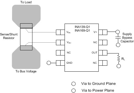
INA139-Q1 INA169-Q1 ai_recommended-layout_sgls185.gif Figure 19. Typical Layout Example