SGLS185F September 2003 – May 2016 INA139-Q1 , INA169-Q1
PRODUCTION DATA.
- 1 Features
- 2 Applications
- 3 Description
- 4 Revision History
- 5 Pin Configuration and Functions
- 6 Specifications
- 7 Detailed Description
-
8 Application and Implementation
- 8.1 Application Information
- 8.2 Typical Applications
- 9 Power Supply Recommendations
- 10Layout
- 11Device and Documentation Support
- 12Mechanical, Packaging, and Orderable Information
6 Specifications
6.1 Absolute Maximum Ratings
over operating free-air temperature range (unless otherwise noted) (1)| MIN | MAX | UNIT | ||||
|---|---|---|---|---|---|---|
| Voltage | Supply, V+ | INA139-Q1 | –0.3 | 60 | V | |
| INA169-Q1 | –0.3 | 75 | V | |||
| Analog inputs, VIN+, VIN– | Common mode | INA139-Q1 | –0.3 | 60 | V | |
| INA169-Q1 | –0.3 | 75 | V | |||
| Differential, (VIN+) – (VIN–) | –40 | 2 | V | |||
| Analog output, OUT | –0.3 | 40 | V | |||
| Temperature | Operating, TA | –55 | 125 | °C | ||
| Junction, TJ | 150 | °C | ||||
| Storage, Tstg | –65 | 150 | °C | |||
(1) Stresses beyond those listed under Absolute Maximum Ratings may cause permanent damage to the device. These are stress ratings only, and functional operation of the device at these or any other conditions beyond those indicated under recommended operating conditions is not implied. Exposure to absolute-maximum-rated conditions for extended periods may affect device reliability.
6.2 ESD Ratings
| VALUE | UNIT | |||
|---|---|---|---|---|
| V(ESD) | Electrostatic discharge | Human-body model (HBM), per AEC Q100-002(1) | ±2000 | V |
| Charged-device model (CDM), per AEC Q100-011 | ±1000 | |||
(1) AEC Q100-002 indicates that HBM stressing shall be in accordance with the ANSI/ESDA/JEDEC JS-001 specification.
6.3 Recommended Operating Conditions
over operating free-air temperature range (unless otherwise noted)| MIN | NOM | MAX | UNIT | ||
|---|---|---|---|---|---|
| Supply voltage, V+ | INA139-Q1 | 2.7 | 5 | 40 | V |
| INA169-Q1 | 2.7 | 5 | 60 | V | |
| Common mode voltage | INA139-Q1 | 2.7 | 12 | 40 | V |
| INA169-Q1 | 2.7 | 12 | 60 | V | |
| Operating temperature, TA | –40 | 125 | °C | ||
6.4 Thermal Information
| THERMAL METRIC(1) | INA1x9-Q1 | UNIT | |
|---|---|---|---|
| PW (TSSOP) | |||
| 8 PINS | |||
| RθJA | Junction-to-ambient thermal resistance | 179.1 | °C/W |
| RθJC(top) | Junction-to-case (top) thermal resistance | 62.6 | °C/W |
| RθJB | Junction-to-board thermal resistance | 107.7 | °C/W |
| ψJT | Junction-to-top characterization parameter | 7 | °C/W |
| ψJB | Junction-to-board characterization parameter | 106 | °C/W |
| RθJC(bot) | Junction-to-case (bottom) thermal resistance | N/A | °C/W |
(1) For more information about traditional and new thermal metrics, see the Semiconductor and IC Package Thermal Metrics application report, SPRA953.
6.5 Electrical Characteristics
at TA = −40°C to +125°C, V+ = 5 V, VIN+ = 12 V, and RL = 25 kΩ (unless otherwise noted)| PARAMETER | TEST CONDITIONS | INA139-Q1 | INA169-Q1 | UNIT | ||||||
|---|---|---|---|---|---|---|---|---|---|---|
| MIN | TYP | MAX | MIN | TYP | MAX | |||||
| INPUT | ||||||||||
| Full-scale sense voltage | VSENSE = VIN+ − VIN− | 100 | 500 | 100 | 500 | mV | ||||
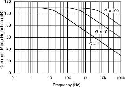
| Common-mode rejection | VIN+ = 2.7 V to 40 V, VSENSE = 50 mV | 100 | 115 | dB | ||||||
| VIN+ = 2.7 V to 60 V, VSENSE = 50 mV | 100 | 120 | ||||||||
| Offset voltage(1) RTI | ±0.2 | ±2 | ±0.2 | ±2 | mV | |||||
| Offset voltage vs temperature | 1 | 1 | μV/°C | |||||||
| Offset voltage vs power supply (V+) | VIN+ = 2.7 V to 40 V, VSENSE = 50 mV | 0.5 | 10 | μV/V | ||||||
| VIN+ = 2.7 V to 60 V, VSENSE = 50 mV | 0.1 | 10 | ||||||||
| Input bias current | 10 | 10 | μA | |||||||
| OUTPUT | ||||||||||
| Transconductance | VSENSE = 10 mV to 150 mV | 980 | 1000 | 1020 | 980 | 1000 | 1020 | μA/V | ||
| Transconductance versus temperature | VSENSE = 100 mV | 10 | 10 | nA/°C | ||||||
| Nonlinearity error | VSENSE = 10 mV to 150 mV | ±0.01% | ±0.2% | ±0.01% | ±0.2% | |||||
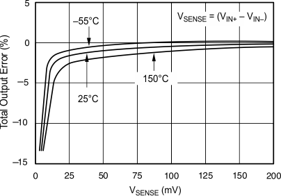
| Total output error | VSENSE = 100 mV | ±0.5% | ±2% | ±0.5% | ±2% | |||||
| Output impedance | 1 || 5 | 1 || 5 | GΩ || pF | |||||||
| Voltage output swing to power supply (V+) | (V+) − 0.9 | (V+) − 1.2 | (V+) − 0.9 | (V+) − 1.2 | V | |||||
| Voltage output swing to common mode, VCM | VCM − 0.6 | VCM − 1 | VCM − 0.6 | VCM − 1 | V | |||||
| FREQUENCY RESPONSE | ||||||||||
| Bandwidth | RL = 10 kΩ | 440 | 440 | kHz | ||||||
| RL = 20 kΩ | 220 | 220 | ||||||||
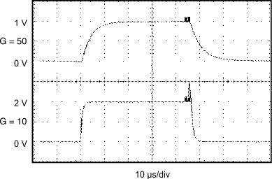
| Settling time (0 1%) | 5 V step, RL = 10 kΩ | 2.5 | 2.5 | μs | ||||||
| 5 V step, RL = 20 kΩ | 5 | 5 | ||||||||
| NOISE | ||||||||||
| Output-current noise density | 20 | 20 | pA/√Hz | |||||||
| Total output-current noise | BW = 100 kHz | 7 | 7 | nA RMS | ||||||
| POWER SUPPLY | ||||||||||
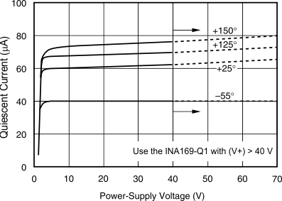
| Quiescent current | VSENSE = 0 V, IO = 0 mA | 60 | 125 | 60 | 125 | μA | ||||
(1) Defined as the amount of input voltage, VSENSE, to drive the output to zero.
6.6 Typical Characteristics
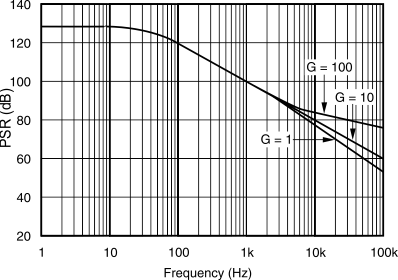
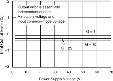
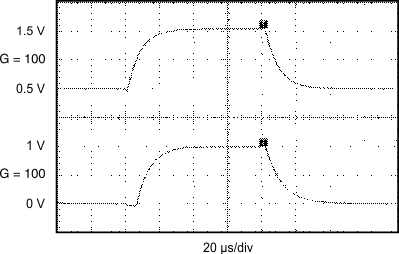
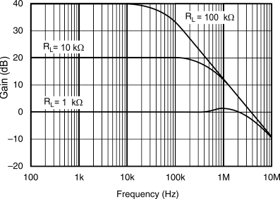
at TA = 25°C, V+ = 5 V, VIN+ = 12 V, and RL = 25 kΩ (unless otherwise noted)