SBOS501F January 2010 – February 2015 INA128-HT , INA129-HT
PRODUCTION DATA.
- 1 Features
- 2 Applications
- 3 Description
- 4 Simplified Schematic
- 5 Revision History
- 6 Pin Configuration and Functions
- 7 Specifications
- 8 Detailed Description
- 9 Application and Implementation
- 10Power Supply Recommendations
- 11Layout
- 12Device and Documentation Support
- 13Mechanical, Packaging, and Orderable Information
封装选项
机械数据 (封装 | 引脚)
散热焊盘机械数据 (封装 | 引脚)
订购信息
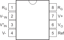
6 Pin Configuration and Functions
D, HKJ, or JDJ Package
8-Pin SOIC, CFP, or CDIP SB
Top View
HKQ Package
8-Pin CFP
Top View
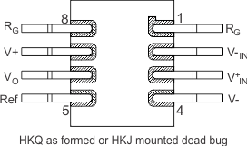
Pin Functions
| PIN | I/O | DESCRIPTION | |
|---|---|---|---|
| NAME | NO. | ||
| Ref | 5 | I | Output voltage reference |
| RG | 1, 8 | O | Gain resistor connection |
| V+ | 7 | Power | Positive power supply voltage from 2.25 V to 18 V |
| V– | 4 | Power | Negative power supply voltage from –2.25 V to –18 V |
| V+IN | 3 | I | Non-inverting input voltage |
| V–IN | 2 | I | Inverting input voltage |
| VO | 6 | O | Output voltage |
Bare Die Information
| DIE THICKNESS | BACKSIDE FINISH | BACKSIDE POTENTIAL | BOND PAD METALLIZATION COMPOSITION |
|---|---|---|---|
| 15 mils | Silicon with backgrind | GND | Al-Si-Cu (0.5%) |
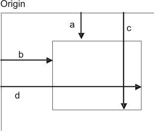
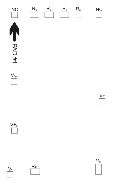
Bond Pad Coordinates in Mils
| DESCRIPTION | PAD NUMBER | a | b | c | d |
|---|---|---|---|---|---|
| NC | 1 | –57.4 | –31.1 | –53.3 | –27 |
| V-IN | 2 | –9.85 | –31.4 | –5.75 | –27.3 |
| V+IN | 3 | 25.05 | –31.4 | 29.15 | –27.3 |
| V- | 4 | 56.2 | –34.3 | 60.3 | –30.2 |
| Ref | 5 | 53.75 | –17.6 | 57.85 | –11 |
| VO | 6 | 50.35 | 27.8 | 56.95 | 31.9 |
| V+ | 7 | 7.75 | 30.2 | 11.85 | 34.3 |
| NC | 8 | –57.4 | 28.4 | –53.3 | 32.5 |
| RG(1) | 9 | –57.4 | 13.4 | –53.3 | 20 |
| RG(1) | 10 | –57.5 | 2.7 | –53.4 | 9.3 |
| RG(1) | 11 | –57.5 | –7.9 | –53.4 | –1.3 |
| RG(1) | 12 | –57.4 | –18.6 | –53.3 | –12 |
(1) Pads 9 and 10 must both be bonded to a common point and correspond to package pin 8. Pads 11 and 12 must both be bonded to a common point and correspond to package pin 1.