ZHCSKE9C December 2015 – October 2019 DS250DF810
PRODUCTION DATA.
- 1 特性
- 2 应用
- 3 说明
- 4 修订历史记录
- 5 说明 (续)
- 6 Pin Configuration and Functions
-
7 Specifications
- 7.1 Absolute Maximum Ratings
- 7.2 ESD Ratings
- 7.3 Recommended Operating Conditions
- 7.4 Thermal Information
- 7.5 Electrical Characteristics
- 7.6 Timing Requirements, Retimer Jitter Specifications
- 7.7 Timing Requirements, Retimer Specifications
- 7.8 Timing Requirements, Recommended Calibration Clock Specifications
- 7.9 Recommended SMBus Switching Characteristics (Slave Mode)
- 7.10 Recommended SMBus Switching Characteristics (Master Mode)
- 7.11 Typical Characteristics
-
8 Detailed Description
- 8.1 Overview
- 8.2 Functional Block Diagram
- 8.3
Feature Description
- 8.3.1 Device Data Path Operation
- 8.3.2 AC-Coupled Receiver and Transmitter
- 8.3.3 Signal Detect
- 8.3.4 Continuous Time Linear Equalizer (CTLE)
- 8.3.5 Variable Gain Amplifier (VGA)
- 8.3.6 Cross-Point Switch
- 8.3.7 Decision Feedback Equalizer (DFE)
- 8.3.8 Clock and Data Recovery (CDR)
- 8.3.9 Calibration Clock
- 8.3.10 Differential Driver with FIR Filter
- 8.3.11 Setting the Output VOD
- 8.3.12 Output Driver Polarity Inversion
- 8.3.13 Debug Features
- 8.3.14 Interrupt Signals
- 8.4 Device Functional Modes
- 8.5 Programming
- 8.6 Register Maps
- 9 Application and Implementation
- 10Power Supply Recommendations
- 11Layout
- 12器件和文档支持
- 13机械、封装和可订购信息
11.2 Layout Example
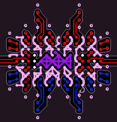
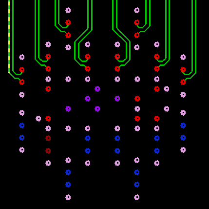
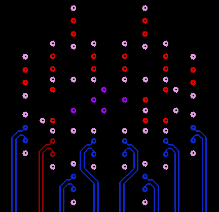
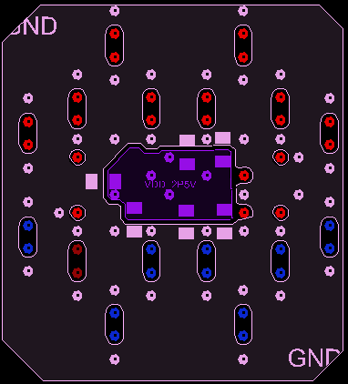
The following example layout demonstrates how all signals can be escaped from the BGA array using stripline routing on a generic 28-layer stackup. This example layout assumes the following:
- Trace width: 0.127 mm (5 mil)
- Trace edge-to-edge spacing: 0.152 mm (6 mil)
- VIA finished hole size (diameter): 0.203 mm (8 mil)
- VIA drilled hole size: 0.254 mm (10 mil)
- VIA-to-VIA spacing: 1.0 mm (39 mil), to enhance PCB manufacturability
- No VIA-in-pad used
Note that many other escape routing options exist using different trace width and spacing combinations. The optimum trace width and spacing will depend on the PCB material, PCB routing density, and other factors.
 Figure 20. Top Layer
  Figure 22. Internal Signal Layer 2
  Figure 21. Internal Signal layer 1
  Figure 23. Bottom Layer