SLVS854E July 2008 – December 2014 DRV8809
PRODUCTION DATA.
- 1 Features
- 2 Applications
- 3 Description
- 4 Revision History
- 5 Pin Configuration and Functions
- 6 Specifications
-
7 Detailed Description
- 7.1 Overview
- 7.2 Functional Block Diagram
- 7.3
Feature Description
- 7.3.1
Serial Interface
- 7.3.1.1 Setup Mode/Power-Down Mode
- 7.3.1.2 Extended Setup Mode
- 7.3.1.3 Serial Interface Timing
- 7.3.1.4 Bipolar Current Regulated Stepper Motor Drive
- 7.3.1.5 Short/Open for Motor Outputs
- 7.3.1.6 DCDC_MODE for Parallel-Mode Control
- 7.3.1.7 DCDC_MODE and C_SELECT Timing Delay and Start-Up Order
- 7.3.1.8 In-Reset: Input for System Reset
- 7.3.1.9 Blanking Time Insertion Timing for DC Motor Driving
- 7.3.2 Motor Driver Configuration
- 7.3.3 Charge Pump
- 7.3.1
Serial Interface
- 7.4 Device Functional Modes
- 7.5 Register Maps
- 8 Application and Implementation
- 9 Power Supply Recommendations
- 10Layout
- 11Device and Documentation Support
- 12Mechanical, Packaging, and Orderable Information
8 Application and Implementation
NOTE
Information in the following applications sections is not part of the TI component specification, and TI does not warrant its accuracy or completeness. TI’s customers are responsible for determining suitability of components for their purposes. Customers should validate and test their design implementation to confirm system functionality.
8.1 Application Information
The DRV8809/DRV8810 provides an integrated motor driver solution. The chip has four H-bridges internally and is configurable to eight different modes of combination motor driver control.
8.2 Typical Application
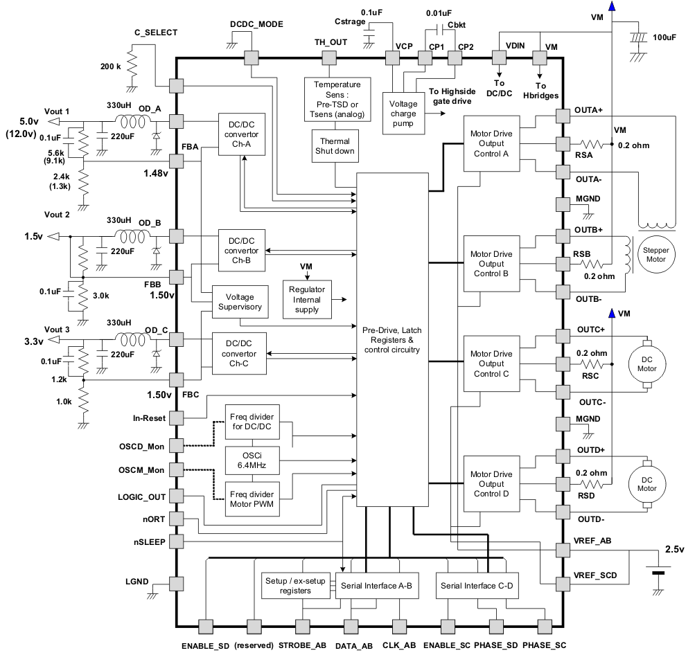 Figure 36. Application Schematic
8.2.1 Design Requirements
To begin the design process, determine the following:
- Output voltage for each DC-DC converters
- Output voltage start up sequence
- Motor configuration (DC motors or stepping motors)
- External Rsense-motor current setting for stepping motor
For one stepper and two DC motor configuration:
- DC-DC Ch-A = 5 V (12 V)
- DC-DC Ch-B = 1.5 V
- DC-DC Ch-C = 3.3 V
If start-up from Ch-B (1.5 V) ≥ Ch-A (5 V), Ch-C 3.3 V should be turned on by the setup register (200 kΩ between C_SELECT pin and GND).
8.2.2 Detailed Design Procedure
8.2.2.1 Output Voltage for Each DC-DC Converter
Output voltage is set by external feedback resistor network. For example,
- 5.0 V Output : 5.6 KΩ and 2.4 KΩ
- 1.5 V Output : 0 Ω and 3.0 KΩ
- 3.3 V Output : 1.2 KΩ and 1.0 KΩ
8.2.2.2 Output Voltage Startup Sequence
DC-DC converters start up sequence is determined by CSELECT pin and DCDC_MODE combination. Refer to the sections DCDC_MODE for Parallel-Mode Control and DCDC_MODE and C_SELECT Timing Delay and Start-Up Order for details.
8.2.2.3 Motor Configuration
Motor configuration is set by SPI register setting. Ramp up device with nSLEEP = Low, then write Setup Register Bits 0 to 3 for motor configuration. Refer to Table 11 for details.
VREF input is typically 2.5V. For example, if Rsense = 5 ohm and Torque (Bit 0 to 1) = 100%
= 500mA
8.2.2.4 External Rsense-Motor Current Setting for Stepping Motor
Stepping motor current level is determined by external Rsense value.
8.2.3 Application Curves
Die temperature can be monitored at TH_OUT pin when register is set as Tsense(analog). This is used for evaluation purposes only. Typical characteristics are shown in Figure 37.
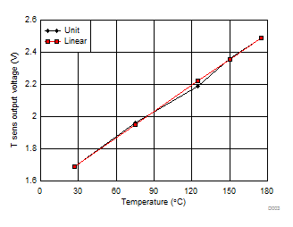 Figure 37. Tsense (Analog Out) Voltage Plot Example