ZHCSCS1D June   2014  – November 2020 DRV8801A-Q1

PRODUCTION DATA  

  1. 特性
  2. 应用
  3. 说明
  4. Revision History
  5. Pin Configuration and Functions
  6. Specifications
    1. 6.1 Absolute Maximum Ratings
    2. 6.2 ESD Ratings
    3. 6.3 Recommended Operating Conditions
    4. 6.4 Thermal Information
    5. 6.5 Electrical Characteristics
    6. 6.6 Dissipation Ratings
    7. 6.7 Typical Characteristics
  7. Detailed Description
    1. 7.1 Overview
    2. 7.2 Functional Block Diagram
    3. 7.3 Feature Description
      1. 7.3.1 Power Supervisor
      2. 7.3.2 Bridge Control
        1. 7.3.2.1 MODE 1
        2. 7.3.2.2 MODE 2
      3. 7.3.3 Fast Decay with Synchronous Rectification
      4. 7.3.4 Slow Decay with Synchronous Rectification (Brake Mode)
      5. 7.3.5 Charge Pump
      6. 7.3.6 SENSE
      7. 7.3.7 VPROPI
        1. 7.3.7.1 Connecting VPROPI Output to ADC
      8. 7.3.8 Protection Circuits
        1. 7.3.8.1 VBB Undervoltage Lockout (UVLO)
        2. 7.3.8.2 Overcurrent Protection (OCP)
        3. 7.3.8.3 Overtemperature Warning (OTW)
        4. 7.3.8.4 Overtemperature Shutdown (OTS)
    4. 7.4 Device Functional Modes
  8. Application and Implementation
    1. 8.1 Application Information
    2. 8.2 Typical Application
      1. 8.2.1 Design Requirements
      2. 8.2.2 Detailed Design Procedure
        1. 8.2.2.1 Drive Current
        2. 8.2.2.2 40
        3. 8.2.2.3 Slow-Decay SR (Brake Mode)
      3. 8.2.3 Thermal Considerations
        1. 8.2.3.1 Junction-to-Ambiant Thermal Impedance (ƟJA)
      4. 8.2.4 Pulse-Width Modulating
        1. 8.2.4.1 Pulse-Width Modulating ENABLE
        2. 8.2.4.2 Pulse-Width Modulating PHASE
      5. 8.2.5 Application Curves
    3. 8.3 Parallel Configuration
      1. 8.3.1 Parallel Connections
      2. 8.3.2 Non – Parallel Connections
      3. 8.3.3 Wiring nFAULT as Wired OR
      4. 8.3.4 Electrical Considerations
        1. 8.3.4.1 Device Spacing
        2. 8.3.4.2 Recirculation Current Handling
        3. 8.3.4.3 Sense Resistor Selection
        4. 8.3.4.4 Maximum System Current
  9. Power Supply Recommendations
    1. 9.1 Bulk Capacitance
  10. 10Layout
    1. 10.1 Layout Guidelines
    2. 10.2 Layout Example
    3. 10.3 Power Dissipation
  11. 11Device and Documentation Support
    1. 11.1 Documentation Support
      1. 11.1.1 Related Documentation
    2. 11.2 Receiving Notification of Documentation Updates
    3. 11.3 支持资源
    4. 11.4 Community Resources
    5. 11.5 Trademarks
    6. 11.6 静电放电警告
    7. 11.7 术语表
  12. 12Mechanical, Packaging, And Orderable Information

封装选项

机械数据 (封装 | 引脚)
散热焊盘机械数据 (封装 | 引脚)
订购信息

Wiring nFAULT as Wired OR

Since nFAULT is an open drain output, multiple nFAULT outputs can be paralleled with a single resistor. The end result is a wired OR configuration. When any individual nFAULT output goes to a logic low, the wired OR output will go to the same logic low. There is no need to determine which device signaled the fault condition, as once they are connected in parallel they function as a single device.
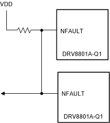
GUID-20201117-CA0I-ZWF2-RXKJ-KCG4TTNB8SL0-low.gif Figure 8-6 nFAULT as Wired OR