SLVSCK2A April 2014 – February 2016 DRV8307
PRODUCTION DATA.
- 1 Features
- 2 Applications
- 3 Description
- 4 Revision History
- 5 Pin Configurations and Functions
- 6 Specifications
-
7 Detailed Description
- 7.1 Overview
- 7.2 Functional Block Diagram
- 7.3 Feature Description
- 7.4 Device Functional Modes
- 8 Application and Implementation
- 9 Power Supply Recommendations
- 10Layout
- 11Device and Documentation Support
- 12Mechanical, Packaging, and Orderable Information
8 Application and Implementation
NOTE
Information in the following applications sections is not part of the TI component specification, and TI does not warrant its accuracy or completeness. TI’s customers are responsible for determining suitability of components for their purposes. Customers should validate and test their design implementation to confirm system functionality.
8.1 Application Information
8.1.1 Hall Sensor Configurations and Connections
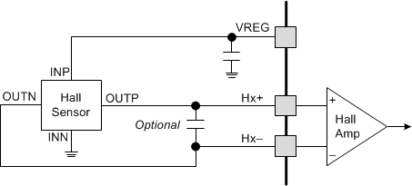
The Hall sensor inputs on the DRV8307 device are capable of interfacing with a variety of Hall sensors. Typically, a Hall element is used, which outputs a differential signal on the order of 100 mV. To use this type of sensor, the VREG regulator can be used to power the Hall sensor. Figure 11 shows the connections.
 Figure 11. Differential Hall Sensor Connections
Since the amplitude of the Hall sensor output signal is very low, often capacitors are placed across the Hall inputs to help reject noise coupled from the motor PWM. Typically capacitors from 1 to 10 nF are used.
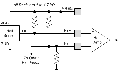
Some motors use digital Hall sensors with open-drain outputs. These sensors can also be used with the DRV8307 device, with the addition of a few resistors (see Figure 12).
 Figure 12. Single-Ended Hall Sensor Connections
The negative (Hx–) inputs are biased to 2.5 V by a pair of resistors between VREG and ground. For open-collector Hall sensors, an additional pullup resistor to VREG is needed on the positive (Hx+) input.
8.1.2 ENABLEn Considerations
Because the ENABLEn function doubles as a sleep (low-power shutdown) function, there are some important considerations when asserting and deasserting ENABLEn.
While the motor driver is enabled, the deassertion of ENABLEn initiates a stop-and-power-down sequence. This sequence starts by disabling the motor (coasting) and waiting for rotation to stop. After rotation is stopped for 1 s (as determined by the absence of transitions on HALLOUT), the internal circuitry is powered-down, the V5 regulator and power switch are disabled, and internal clocks are stopped.
After this stop-and-power-down sequence has been initiated (by deasserting the ENABLEn terminal for at least 1.2 μs), the sequence continues to completion, regardless of the state of ENABLEn.
8.1.3 Faster Starting and Stopping
When the DRV8307 is spinning a motor and ENABLEn is brought high while BRAKE is left low, the external MOSFETs is disabled and the motor coasts to a stop. The motor cannot be re-driven until it first completely stops.
For more dynamic performance, the ENABLEn and BRAKE inputs can be tied together. Then when the motor is disabled (by bringing ENABLEn high), BRAKE is also high, causing the low-side of each half-H bridge to be on. This causes the motor to stop faster, and allows it to be re-driven sooner.
8.2 Typical Application
8.2.1 Design Requirements
| Design Parameter | Value |
|---|---|
| Supply voltage | 8.5 to 32 V |
| PWM frequency | 16 to 50 kHz |
| PWM duty cycle | 0% to 100% |
| Current limiter | VLIMITER / RISENSE |
| External FETs | N-channel MOSFETs |
| Bulk supply capacitance | 2 to 4 µF per watt |
8.2.2 Detailed Design Procedure
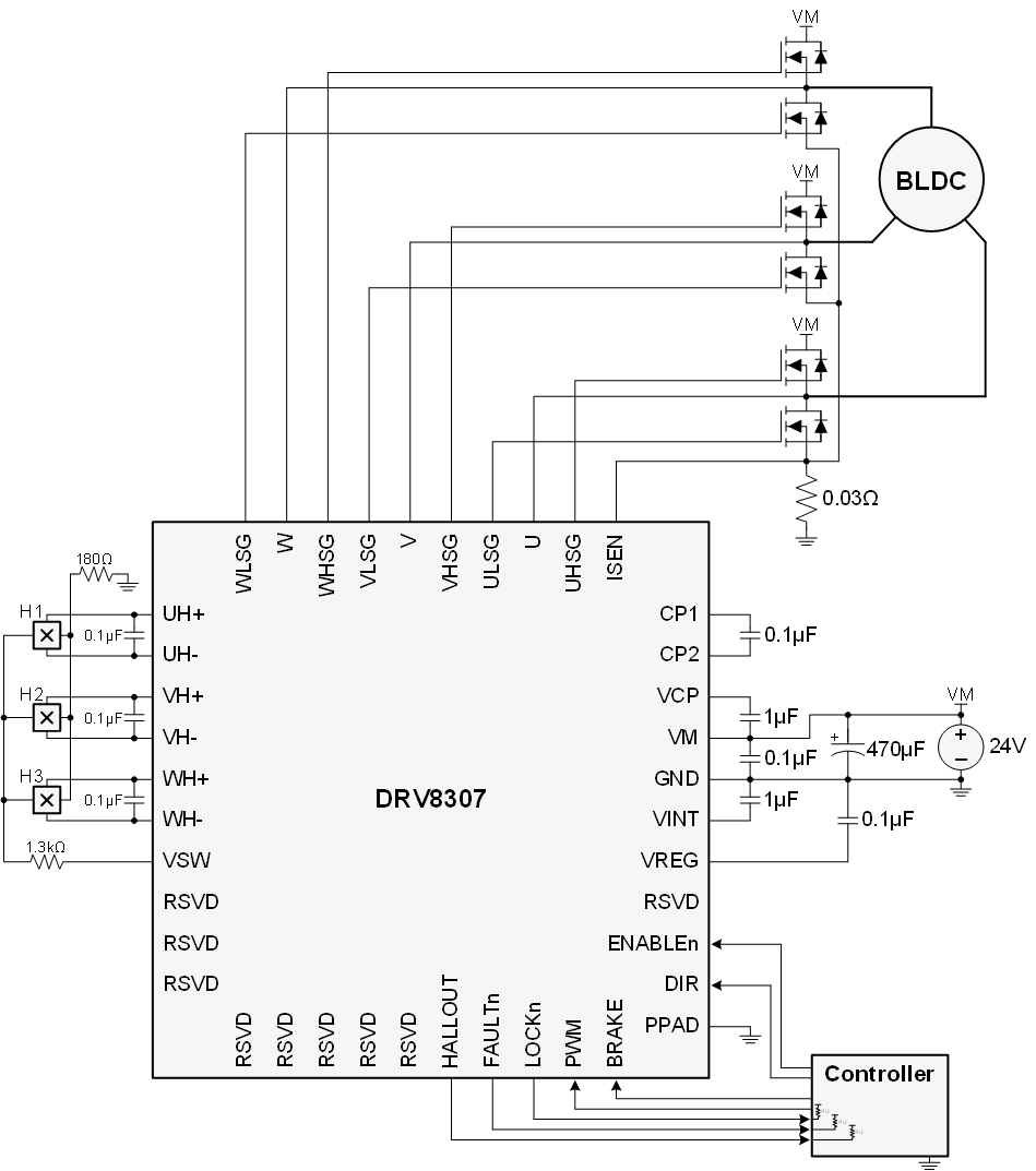
When designing a system with the DRV8307, determine an operating motor voltage between 8.5 to 32 V. Higher voltages directly scale motor speed, with the same PWM input.
The frequency of the input clock (PWM) must be between 16 and 50 kHz. Note that this frequency does not affect the pre-driver output frequency, which is fixed at 25 kHz (typical).
The PWM duty cycle controls motor speed and can be set either to a fixed value or varied while the motor is spinning. If it is changed while spinning, use gradual steps (for example, 1% increments), because a large change in the commanded duty cycle can cause a large step in commutation, which can lock up the motor. This behavior is typical with other industry devices.
The DRV8307 device constantly monitors motor current and reduces FET drive when necessary, to keep current within VLIMITER / RISENSE. This feature reduces the requirements of power supply current capacity and bulk capacitance to maintain a stable voltage, especially during motor startup. The designer should target a peak current limit and size RISENSE appropriately. VLIMITER is fixed at 0.25 V (typical).
For example, if 4-A peak is desired, then a 0.06-Ω resistor should be chosen as in Equation 2.
When selecting the power FETs, use six N-channel MOSFETs. They must support VGS > 10 V (since the DRV8307 device drives 10 V VGS). They must also support VDS > VM, and TI recommends to have 1.5× to 2× margin, to prevent FET damage during transient voltage spikes that can occur when motors change speeds.
It is important to use large bulk capacitance on VM, and the required size depends on the power of the motor. Of course, power = voltage × current. A general recommendation is to use 2 to 4 µF per watt. If a motor system uses 24 V and 3 A, a reasonable choice is 144 to 288 µF.
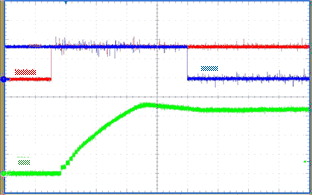
8.2.3 Application Performance Plot

