SLOS719F August 2011 – January 2016 DRV8301
PRODUCTION DATA.
- 1 Features
- 2 Applications
- 3 Description
- 4 Revision History
- 5 Pin Configuration and Functions
-
6 Specifications
- 6.1 Absolute Maximum Ratings
- 6.2 Recommended Operating Conditions
- 6.3 Thermal Information
- 6.4 Electrical Characteristics
- 6.5 Current Shunt Amplifier Characteristics
- 6.6 Buck Converter Characteristics
- 6.7 SPI Timing Requirements (Slave Mode Only)
- 6.8 Gate Timing and Protection Switching Characteristics
- 6.9 Typical Characteristics
- 7 Detailed Description
- 8 Application and Implementation
- 9 Power Supply Recommendations
- 10Layout
- 11Device and Documentation Support
- 12Mechanical, Packaging, and Orderable Information
10 Layout
10.1 Layout Guidelines
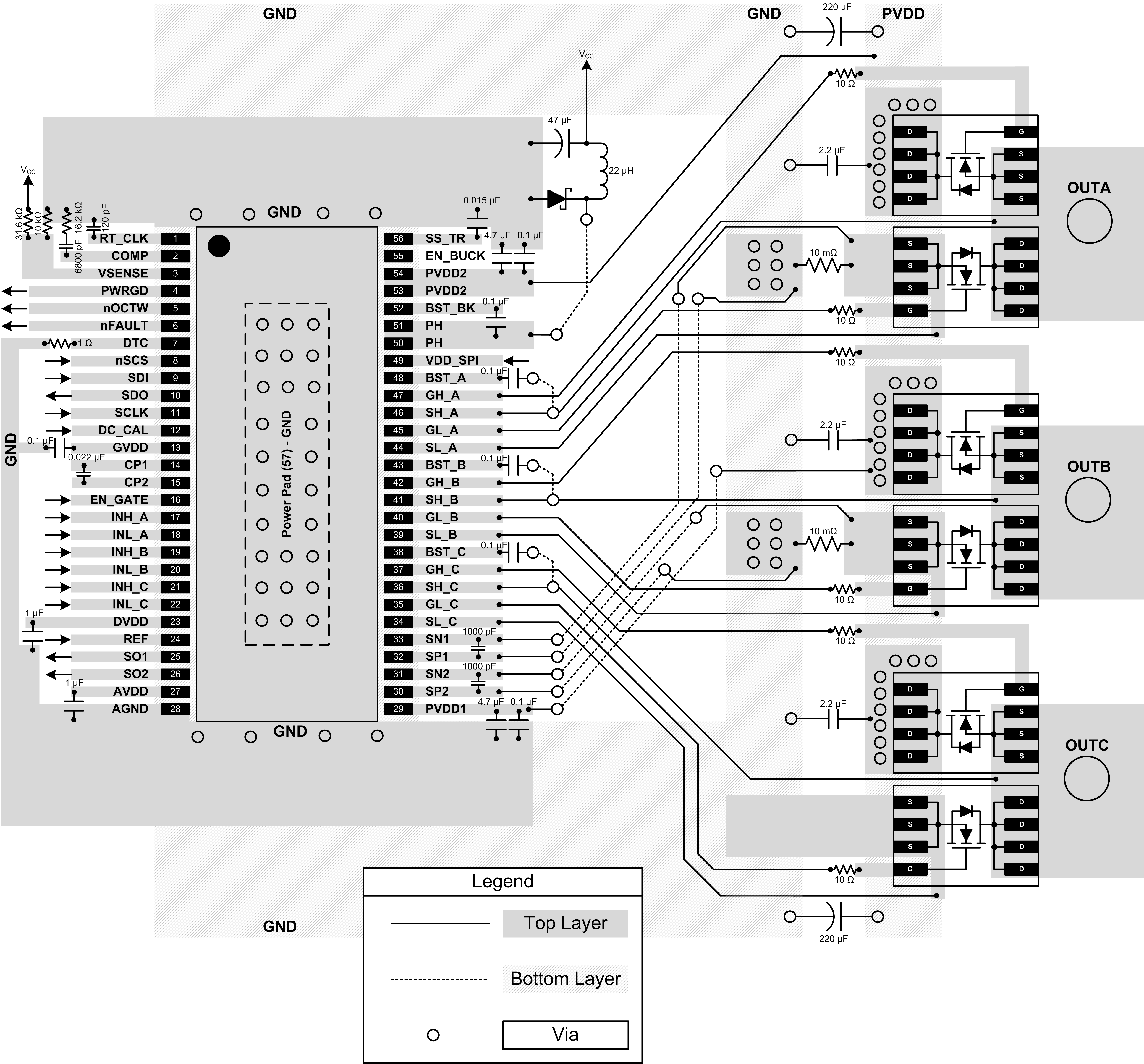
Use these layout recommendations when designing a PCB for the DRV8301.
- The DRV8301 makes an electrical connection to GND through the PowerPAD. Always check to ensure that the PowerPAD has been properly soldered (See PowerPAD™ Thermally Enhanced Package application report, SLMA002).
- PVDD bypass capacitors should be placed close to their corresponding pins with a low impedance path to device GND (PowerPAD).
- GVDD bypass capacitor should be placed close its corresponding pin with a low impedance path to device GND (PowerPAD).
- AVDD and DVDD bypass capacitors should be placed close to their corresponding pins with a low-impedance path to the AGND pin. It is preferable to make this connection on the same layer.
- AGND should be tied to device GND (PowerPAD) through a low impedance trace/copper fill.
- Add stitching vias to reduce the impedance of the GND path from the top to bottom side.
- Try to clear the space around and underneath the DRV8301 to allow for better heat spreading from the PowerPAD.
10.2 Layout Example
 Figure 13. Top and Bottom Layer Layout Schematic