ZHCSEF3G May   2014  – September 2016 DRV5023

PRODUCTION DATA.  

  1. 特性
  2. 应用
  3. 说明
  4. 修订历史记录
  5. Pin Configuration and Functions
  6. Specifications
    1. 6.1 Absolute Maximum Ratings
    2. 6.2 ESD Ratings
    3. 6.3 Recommended Operating Conditions
    4. 6.4 Thermal Information
    5. 6.5 Electrical Characteristics
    6. 6.6 Switching Characteristics
    7. 6.7 Magnetic Characteristics
    8. 6.8 Typical Characteristics
  7. Detailed Description
    1. 7.1 Overview
    2. 7.2 Functional Block Diagram
    3. 7.3 Feature Description
      1. 7.3.1 Field Direction Definition
      2. 7.3.2 Device Output
      3. 7.3.3 Power-On Time
      4. 7.3.4 Output Stage
      5. 7.3.5 Protection Circuits
        1. 7.3.5.1 Overcurrent Protection (OCP)
        2. 7.3.5.2 Load Dump Protection
        3. 7.3.5.3 Reverse Supply Protection
    4. 7.4 Device Functional Modes
  8. Application and Implementation
    1. 8.1 Application Information
    2. 8.2 Typical Applications
      1. 8.2.1 Standard Circuit
        1. 8.2.1.1 Design Requirements
        2. 8.2.1.2 Detailed Design Procedure
          1. 8.2.1.2.1 Configuration Example
        3. 8.2.1.3 Application Curves
      2. 8.2.2 Alternative Two-Wire Application
        1. 8.2.2.1 Design Requirements
        2. 8.2.2.2 Detailed Design Procedure
  9. Power Supply Recommendations
  10. 10Layout
    1. 10.1 Layout Guidelines
    2. 10.2 Layout Example
  11. 11器件和文档支持
    1. 11.1 器件支持
      1. 11.1.1 器件命名规则
      2. 11.1.2 器件标记
    2. 11.2 接收文档更新通知
    3. 11.3 社区资源
    4. 11.4 商标
    5. 11.5 静电放电警告
    6. 11.6 Glossary
  12. 12机械、封装和可订购信息

封装选项

机械数据 (封装 | 引脚)
散热焊盘机械数据 (封装 | 引脚)
订购信息

5 Pin Configuration and Functions

For additional configuration information, see 器件标记 and 机械、封装和可订购信息.

DBZ Package
3-Pin SOT-23
Top View
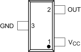
DRV5023 po_sot_slis150.gif
LPG Package
3-Pin TO-92
Top View
DRV5023 LPG-3_Pinout_Top_View.gif

Pin Functions

PIN TYPE DESCRIPTION
NAME DBZ LPG
GND 3 2 GND Ground pin
OUT 2 3 Output Hall sensor open-drain output. The open drain requires a resistor pullup.
VCC 1 1 Power 2.5 to 38 V power supply. Bypass this pin to the GND pin with a 0.01-μF (minimum) ceramic capacitor rated for VCC.