ZHCSDW9B May 2015 – March 2016 DRV421
PRODUCTION DATA.
- 1 特性
- 2 应用
- 3 说明
- 4 修订历史记录
- 5 Pin Configuration and Functions
- 6 Specifications
-
7 Detailed Description
- 7.1 Overview
- 7.2 Functional Block Diagram
- 7.3
Feature Description
- 7.3.1 Fluxgate Sensor
- 7.3.2 Integrator-Filter Function and Compensation Loop Stability
- 7.3.3 H-Bridge Driver for Compensation Coil
- 7.3.4 Shunt Sense Amplifier
- 7.3.5 Overrange Comparator
- 7.3.6 Voltage Reference
- 7.3.7 Overload Detection and Control
- 7.3.8 Magnetic Core Demagnetization
- 7.3.9 Search Function
- 7.3.10 Error Flag
- 7.4 Device Functional Modes
- 8 Application and Implementation
- 9 Power-Supply Recommendations
- 10Layout
- 11器件和文档支持
- 12机械、封装和可订购信息
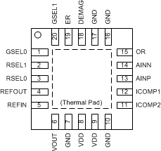
5 Pin Configuration and Functions
Pin Functions
| PIN | I/O | DESCRIPTION | |
|---|---|---|---|
| NAME | NO. | ||
| AINN | 14 | I | Inverting input of shunt sense amplifier |
| AINP | 13 | I | Noninverting input of shunt sense amplifier |
| DEMAG | 18 | I | Degauss control input |
| ER | 19 | O | Error flag; open-drain, active low output |
| GND | 7, 10, 16, 17 | — | Ground reference |
| GSEL0 | 1 | I | Gain and bandwidth selection input 0 |
| GSEL1 | 20 | I | Gain and bandwidth selection input 1 |
| ICOMP1 | 12 | O | Output 1 of compensation coil driver |
| ICOMP2 | 11 | O | Output 2 of compensation coil driver |
| OR | 15 | O | Shunt sense amplifier overrange indicator; open-drain, active-low output |
| REFIN | 5 | I | Common-mode reference input for the shunt sense amplifier |
| REFOUT | 4 | O | Voltage reference output |
| RSEL0 | 3 | I | Voltage reference mode selection input 0 |
| RSEL1 | 2 | I | Voltage reference mode selection input 1 |
| VDD | 8, 9 | — | Supply voltage, 3.0 V to 5.5 V. Decouple both pins using 1-µF ceramic capacitors placed as close as possible to the device. See the Power-Supply Decoupling and Layout sections for further details. |
| VOUT | 6 | O | Shunt sense amplifier output |
| PowerPAD™ | — | Connect thermal pad to GND | |
