SLVSCE5B November 2013 – July 2016 DRV3203E-Q1
- 1 Features
- 2 Applications
- 3 Description
- 4 Revision History
- 5 Pin Configuration and Functions
- 6 Specifications
-
7 Detailed Description
- 7.1 Functional Block Diagram
- 7.2 Feature Description
- 7.3
Register Maps
- 7.3.1
Register Descriptions
- 7.3.1.1 CFGUNLK (address 0x01): Configuration Unlock Register
- 7.3.1.2 FLTCFG (address 0x02): Fault Detection Configuration Register
- 7.3.1.3 FLTEN0 (address 0x04): FAULT Pin Enable Register 0
- 7.3.1.4 FLTEN1 (address 0x05): FAULT Pin Enable Register 1
- 7.3.1.5 SDNEN0 (address 0x06): Pre-Driver Shutdown Enable Register 0
- 7.3.1.6 SDNEN1 (address 0x07): Pre-Driver Shutdown Enable Register 1
- 7.3.1.7 FLTFLG0 (address 0x08): Fault Flag Register 0
- 7.3.1.8 FLGFLT1 (address 0x09): Fault Flag Register 1
- 7.3.1.9 CSCFG (address 0x0A): Current Sense Configuration Register
- 7.3.1.10 PDCFG (address 0x0B): Pre-Driver Configuration Register
- 7.3.1.11 DIAG (address 0x0C): Diagnosis Register
- 7.3.1.12 SPARE (address 0x0D): Spare Register
- 7.3.1
Register Descriptions
- 8 Application and Implementation
- 9 Device and Documentation Support
- 10Mechanical, Packaging, and Orderable Information
6 Specifications
6.1 Absolute Maximum Ratings
over operating free-air temperature range (unless otherwise noted)| MIN | MAX | UNIT | |||
|---|---|---|---|---|---|
| TA | Operating temperature range | –40 | 150 | ºC | |
| TJ | Junction temperature | –40 | 175 | ºC | |
| Tstg | Storage temperature | –55 | 175 | ºC | |
6.2 ESD Ratings
| VALUE | UNIT | |||
|---|---|---|---|---|
| V(ESD) | Electrostatic discharge | Human-body model (HBM), per AEC Q100-002(1) | ±2000 | V |
| Charged-device model (CDM), per AEC Q100-011 | ±500 | |||
(1) AEC Q100-002 indicates that HBM stressing shall be in accordance with the ANSI/ESDA/JEDEC JS-001 specification.
6.3 Thermal Information
| THERMAL METRIC | DRV3203E-Q1 | UNIT | |
|---|---|---|---|
| PHP (HTQFP) | |||
| 48 PINS | |||
| θJA | Junction-to-ambient thermal resistance | 26.1 | °C/W |
| θJCtop | Junction-to-case (top) thermal resistance | 11.5 | °C/W |
| θJB | Junction-to-board thermal resistance | 7.2 | °C/W |
| ψJT | Junction-to-top characterization parameter | 0.2 | °C/W |
| ψJB | Junction-to-board characterization parameter | 7.1 | °C/W |
| θJCbot | Junction-to-case (bottom) thermal resistance | 0.4 | °C/W |
6.4 Electrical Characteristics
VB = 12 V, TA = –40°C to +150℃ (unless otherwise specified)| PARAMETER | TEST CONDITIONS | MIN | TYP | MAX | UNIT | |
|---|---|---|---|---|---|---|
| WATCHDOG | ||||||
| VSTN(1) | Function start VCC voltage RES | See Figure 1 | - | 0.8 | 1.3 | V |
| tON(1) | Power-on time RES | 2.5 | 3 | 3.5 | ms | |
| tOFF(1) | Clock-off reset time RES | 64 | 80 | 96 | ms | |
| tRL(1) | Reset-pulse low time RES | 16 | 20 | 24 | ms | |
| tRH(1) | Reset-pulse high time RES | 64 | 80 | 96 | ms | |
| tRES(1) | Reset delay time RES | 30 | 71.5 | 90 | µs | |
| Pwth(1) | Pulse duration PRN | 2 | - | - | µs | |
| SPI | ||||||
| fop | SPI clock frequency | - | 4 | MHz | ||
| tlead(1) | Enable lead time | 200 | - | - | ns | |
| twait(1) | Wait time between two successive communications | 5 | - | - | µs | |
| tlag(1) | Enable lag time | 100 | - | - | ns | |
| tpw(1) | SCLK pulse duration | 100 | - | - | ns | |
| tsu(1) | Data setup time | 100 | - | - | ns | |
| th(1) | Data hold time | 100 | - | - | ns | |
| tdis(1) | Data-output disable time | - | - | 200 | ns | |
| ten(1) | Data-output enable time | - | - | 100 | ns | |
| td (1) | Data delay time, SCK to DOUT | CL = 50 pF, see Figure 2. | 0 | - | 100 | ns |
| CHARGE PUMP | ||||||
| Vchv1_0 | Output voltage, PDCPV | VB = 5.3 V, load = 0 mA, C1 = C2 = 47 nF, CCP = 2.2 µF, R1 = R2 = 0 Ω |
VB + 7 | VB + 8 | - | V |
| Vchv1_1 | Output voltage, PDCPV | VB = 5.3 V, Ioad = 5 mA, C1 = C2 = 47 nF, CCP = 2.2 µF, R1 = R2 = 0 Ω |
VB + 5.5 | VB + 6.5 | - | V |
| Vchv1_2 | Output voltage, PDCPV | VB = 5.3 V, Ioad = 8 mA, C1 = C2 = 47 nF, CCP = 2.2 µF, R1 = R2 = 0 Ω |
VB + 4.5 | VB + 5.5 | - | V |
| Vchv2_0 | Output voltage, PDCPV | VB = 12 V, Ioad = 0 mA, C1 = C2 = 47 nF, CCP = 2.2 µF, R1 = R2 = 0 Ω |
VB + 10 | VB + 12 | VB + 14 | V |
| Vchv2_1 | Output voltage, PDCPV | VB = 12 V, Ioad = 11 mA, C1 = C2 = 47 nF, CCP = 2.2 µF, R1 = R2 = 0 Ω |
VB + 9.5 | VB + 11.5 | VB + 13.5 | V |
| Vchv2_2 | Output voltage, PDCPV | VB = 12 V, Ioad = 18 mA, C1 = C2 = 47 nF, CCP = 2.2 µF, R1 = R2 = 0 Ω |
VB + 9 | VB + 11 | VB + 13 | V |
| Vchv3_0 | Output voltage, PDCPV | VB = 18 V, Ioad = 0 mA, C1 = C2 = 47 nF, CCP = 2.2 µF, R1 = R2 = 0 Ω |
VB + 10 | VB + 12 | VB + 14 | V |
| Vchv3_1 | Output voltage, PDCPV | VB = 18 V, Ioad = 13 mA, C1 = C2 = 47 nF, CCP = 2.2 µF, R1 = R2 = 0 Ω |
VB + 10 | VB + 12 | VB + 14 | V |
| Vchv3_2 | Output voltage, PDCPV | VB = 18 V, Ioad = 22 mA, C1 = C2 = 47 nF, CCP = 2.2 µF, R1 = R2 = 0 Ω |
VB + 10 | VB + 12 | VB + 14 | V |
| VchvOV | Overvoltage detection threshold | 35 | 37.5 | 40 | V | |
| VchvUV | Undervoltage detection threshold | VB + 4 | VB + 4.5 | VB + 5 | V | |
| tchv(1) | Rise time | VB = 5.3 V, C1 = C2 = 47 nF, CCP = 2.2 µF, R1 = R2 = 0 Ω, Vchv, UV released |
1 | 2 | ms | |
| Ron | On-resistance, S1-S4 | See Figure 10 | 8 | Ω | ||
| HIGH-SIDE PRE-DRIVER | ||||||
| VOH_H | Output voltage, turnon side | Isink = 10 mA, PDCPV - xH | 1.35 | 2.7 | V | |
| VOL_H | Output voltage, turnoff side | Isource = 10 mA, xH - xHS | 25 | 50 | mV | |
| RONH_HP | On-resistance, turnon side (Pch) | U(V/W)H = PDCPV - 1 V | 135 | 300 | Ω | |
| RONH_HN | On-resistance, turnon side (Nch) | U(V/W)H = PDCPV - 2.5 V | 4 | 8 | Ω | |
| RONL_H | On-resistance turnoff side | 2.5 | 5 | Ω | ||
| ton_h(1) | Turnon time | CL = 12 nF, RL = 0 Ω from 20% to 80% | 50 | - | 200 | ns |
| toff_h(1) | Turnoff time | CL = 12 nF, RL = 0 Ω from 80% to 20% | 50 | - | 200 | ns |
| th-ondly(1) | Output delay time | CL = 12 nF, RL = 0 Ω to 20%, no dead time | - | 200 | - | ns |
| th-offdly(1) | Output delay time | CL = 12 nF, RL = 0 Ω to 80%, no dead time | - | 200 | - | ns |
| VGS_hs | Gate-source high -side voltage difference | xH-xHS | –0.3 | 18 | V | |
| LOW-SIDE PRE-DRIVER | ||||||
| VOH_L1 | Output voltage, turnon side | VB = 12 V, Isink = 10 mA, xL -NGND | 10 | 12 | 14 | V |
| VOH_L2 | Output voltage, turnon side | VB = 5.3 V, Isink = 10 mA, xL - NGND | 5.5 | 7.5 | 10 | V |
| VOL_L | Output voltage, turnoff side | Isource = 10 mA, xL - NGND | - | 25 | 60 | mV |
| RONH_L | On-resistance, turnon side | - | 6 | 12 | Ω | |
| RONL_L | On-resistance, turnoff side | 2.5 | 6 | Ω | ||
| ton_l (1) | Turnon time | CL = 18 nF, RL = 0 Ω, from 20% to 80% of 12 V, from 20% to 80% of 6 V (VB = 5.3 V) |
50 | - | 200 | ns |
| t off_l (1) | Turnoff time | CL = 18 nF, RL = 0 Ω, from 80% to 20% of 12 V, from 80% to 20% of 6 V (VB = 5.3 V) |
50 | - | 200 | ns |
| tl-ondly(1) | Output delay time | CL = 18 nF, RL = 0 Ω, to 20% of 12 V, to 20% of VOH = 6 V (VB = 5.3 V), no dead time |
- | 200 | - | ns |
| tl-offdly(1) | Output delay time | CL = 18 nF, RL = 0 Ω, to 80% of 12 V, to 80% of VOH = 6 V (VB = 5.3 V), no dead time |
- | 200 | - | ns |
| tdiff1(1) | Differential time1 | (Th-on) - (Tl-off), no dead time, See Figure 3 |
–200 | 0 | 200 | ns |
| tdiff2(1) | Differential time2 | (Tl-on) - (Tl-off), no dead time, See Figure 3 |
–200 | 0 | 200 | ns |
| tdead(1) | Dead time | OSC1 = 10 MHz SPI register PDCFG.DEADT | 2 1.5 1 0.5 |
2.2 1.7 1.2 0.7 |
µs | |
| PHASE COMPARTOR | ||||||
| VIOfs | Input offset voltage | –15 | - | 15 | mV | |
| VIm1 | Input voltage range, PHTM | VB = 6 V – 26.5 V | 1.3 | - | 4.5 | V |
| VIm2 | Input voltage range, PHTM | VB = 5.3 V | 1.3 | - | 4.2 | V |
| VIp | Input voltage range, PHxM | –1 | - | VB | V | |
| Vhys | Threshold hysteresis voltage | SPI register SPARE. SEL_COMP_HYS | - | 0 | - | mV |
| 12.5 | 25 | 50 | ||||
| 25 | 50 | 100 | ||||
| 50 | 100 | 200 | ||||
| VOH | Output high voltage | Isink = 2.5 mA | 0.9 × VCC | - | - | V |
| VOL | Output low voltage | Isource = 2.5 mA | - | - | 0.1 × VCC | V |
| tres_tr(1) | Response time, rising | CL = 100 pF | - | 0.7 | 1.5 | µs |
| tres_tf(1) | Response time, falling | CL = 100 pF | - | 0.7 | 1.5 | µs |
| MOTOR CURRENT SENSE | ||||||
| VOfs | Input offset voltage | –5 | 5 | mV | ||
| VO_0 | Output voltage, ALV | Imotor = 0 A, SPI register CSCFG. CSOFFSET | - | 0.5 1 1.5 |
- | V |
| VLine | Linearity, ALV | Rshunt = 1 mΩ, R11 = R12 = 1 kΩ, R21 = R22 = 30 kΩ |
29.4 | 30 | 30.6 | mV/A |
| VGain | Gain | 10 | 30 | - | V/V | |
| Tset_TR1(1) | Settling time (rise), ALV ±1% | Rshunt = 1 mΩ, VGain = 30, CL = 100 pF, Imotor = 0 A → 30 A, (ALV: 1 V → 1.9 V, AREF = 1 V) |
- | 1 | 2.5 | µs |
| Tset_TR2(1) | Settling time(rise), ALV ±1% | Rshunt = 1 mΩ, VGain = 30, CL = 100 pF, Imotor = 0 A → 60 A, (ALV: 1 V → 2.8 V, AREF = 1 V) |
- | 1 | 2.5 | µs |
| Tset_TF1(1) | Settling time(fall), ALV ±1% | Rshunt = 1 mΩ, VGain = 30, CL = 100 pF, Imotor = 30 A → 0, (ALV: 1.9 V → 1 V, AREF = 1 V) |
- | 1 | 2.5 | µs |
| Tset_TF2(1) | Settling time(fall), ALV ±1% | Rshunt = 1 mΩ, VGain = 30, CL = 100 pF, Imotor = 60 A → 0, (ALV: 2.8 V → 1 V, AREF = 1 V) |
- | 1 | 2.5 | µs |
| OVADth | Overcurrent threshold | Rshunt = 1 mΩ, VGain = 30, AREF = 1 V, ADTH = 1.98 V, SPI register FLTCFG. MTOCTH, OVADth = (2 × ADTH -- AREF) / (Rshunt × VGain) |
89.1 | 99 | 108.9 | A |
| TDEL_OVAD(1) | Propagation delay (rise or fall) |
- | - | 1.5 | µs | |
| tfiltMTOC | filtering time | OSC1 = 9 MHz-11 MHz | 0.8 | 1 | 1.2 | µs |
| VCC | ||||||
| VCC1 | Output Voltage | 3.23 | 3.3 | 3.37 | V | |
| IBVCC | Base Current | 2 | mA | |||
| hfePNP | DC current gain of external PNP | 100 | - | - | ||
| VLRVCC | Load regulation | ILVCC = 5 mA to 200 mA | -20 | - | 20 | mV |
| CVCC | External Capacitance | 22 | 100 | µF | ||
| RVCC | ESR of external Capacitor | 300 | mΩ | |||
| VCCUV | Under voltage detection threshold | SPI register FLTCFG. VCCUVTH | 2 2.2 |
2.2 2.4 |
2.4 2.6 |
V |
| VCCUVHYS | Under voltage detection threshold hysteresis | 33 | 66 | 132 | mV | |
| VCCOV | Overvoltage detection threshold | 3.5 | 3.8 | 4.1 | V | |
| VCCOC | Current Limit | Rsns = 0.51 Ω, 0.2 V ⋍ Rsns x VCCOC | 300 | 400 | 550 | mA |
| Tvcc1(1) | Rise Time | VCC > VCCUV, CVCC = 22 µF | 0.5 | ms | ||
| Tvcc2(1) | Rise Time | VCC > VCCUV, CVCC = 100 µF | 1.5 | ms | ||
| VDD | ||||||
| VDD | Output Voltage | 3 | 3.3 | 3.6 | V | |
| CVDD | Load Capacitance | 1 | µF | |||
| VDDUV | Under voltage detection threshold | 2.1 | 2.3 | 2.5 | V | |
| VDDOV | Overvoltage detection threshold | 4 | 4.3 | 4.6 | V | |
| Tvdd(1) | Rise Time | VDD > VDDUV, CVDD = 1 µF | 100 | µs | ||
| VB MONITOR | ||||||
| VBOV | VB overvoltage detection threshold level | 26.5 | 27.5 | 28.5 | V | |
| VBUV | VB Undervoltage detection threshold level | SPI register FLTCFG. VBUVTH | 3.65 4.15 4.65 5.15 |
4 4.5 5 5.5 |
4.35 4.85 5.35 5.85 |
V |
| THERMAL SHUT DOWN | ||||||
| TSD(1) | Thermal shut down threshold level | 155 | 175 | 195 | °C | |
| TSDhys(1) | Thermal shut down hysteresis | 5 | 10 | 15 | °C | |
| OSCILLATOR | ||||||
| OSC1 | OSC1 frequency | 9 | 10 | 11 | MHz | |
| OSC2 | OSC2 frequency | 10 | MHz | |||
| INPUT BUFFER1 | ||||||
| VIH | Input threshold logic high | 0.7 × VCC | V | |||
| VIL | Input threshold logic low | 0.3 × VCC | V | |||
| Ru or Rd | Input pullup or pulldown resistance | 50 | 100 | 150 | kΩ | |
| OUTPUT BUFFER1(2) | ||||||
| VOH | Output level logic high | Isink = 1 mA | 0.9 × VCC | V | ||
| VOL | Output level logic low | Isource = 1 mA | 0.1 × VCC | V | ||
| OUTPUT BUFFER3 | ||||||
| R_RES | Pull up Resistor | 2 | 3 | 4 | kΩ | |
| VOL | Output level logic low | Isource = 2 mA | 0.1 × VCC | V | ||
(1) Specified by design.
6.5 Supply Voltage and Current
VB = 12 V, TA = –40°C to +150°C (unless otherwise specified)| PARAMETER | TEST CONDITIONS | MIN | TYP | MAX | UNITS | |
|---|---|---|---|---|---|---|
| SUPPLY INPUT | ||||||
| VB1(1) | VB supply voltage (motor operation) | Full device functionality | 5.3 | 12 | 18 | V |
| VB2(1) | VB supply voltage (MCU operation) | Full device functionality | 4.5 | 12 | 18 | V |
| VB3(2) | VB supply voltage | 18 | - | 26.5 | V | |
| Ivb | VB operating current | ENABLE = High, no PWM | - | 18 | 27 | mA |
| Ivbq | VB quiescent current | ENABLE = Low | - | 50 | 100 | µA |
(1) Performance of supply voltage 5.3 to 18 V is according to the ACE-Q100 (Grade 0) standard.
(2) Specified by design.
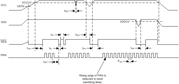
NOTE:
VCC undervoltage condition sets RES = Low.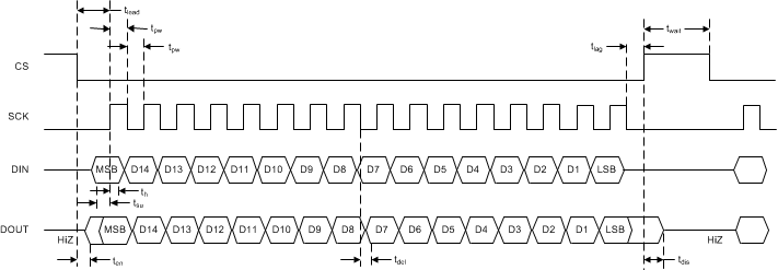 Figure 2. SPI Timing Diagram

NOTE:
This diagram excludes dead time to explain the timing parameters of the pre-driver.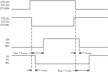 Figure 4. Dead Time
 Figure 5. Motor Current Sense and Overcurrent
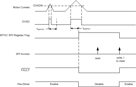
1. MCU must set the FLTCFG.FLGLATCH_EN bit to 1 to get the latch-type operation shown in this figure.
2. When MTOC condition is detected, FAULT is asserted to low if FE_MTOC bit is 1.
3. When MTOC condition is detected, Pre Driver is disabled if SE_MTOC is 1.
Figure 6. Motor Overcurrent Event
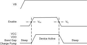 Figure 7. I/O ENABLE Timing Chart