SNOSAX1F May 2008 – September 2015 DP83849I
PRODUCTION DATA.
- 1 Device Overview
- 2 Revision History
- 3 Terminal Configuration and Functions
- 4 Specifications
-
5 Detailed Description
- 5.1 Overview
- 5.2 Functional Block Diagram
- 5.3 Feature Description
- 5.4 Device Functional Modes
- 5.5
Programming
- 5.5.1 Architecture
- 5.5.2 100BASE-TX Receiver
- 5.5.3
Analog Front End
- 5.5.3.1 Digital Signal Processor
- 5.5.3.2 Digital Adaptive Equalization and Gain Control
- 5.5.3.3 Signal Detect
- 5.5.3.4 MLT-3 to NRZI Decoder
- 5.5.3.5 NRZI to NRZ
- 5.5.3.6 Serial to Parallel
- 5.5.3.7 Descrambler
- 5.5.3.8 Code-Group Alignment
- 5.5.3.9 4B/5B Decoder
- 5.5.3.10 100BASE-TX Link Integrity Monitor
- 5.5.3.11 BAD SSD Detection
- 5.5.4
10BASE-T Transceiver Module
- 5.5.4.1 Operational Modes
- 5.5.4.2 Smart Squelch
- 5.5.4.3 Collision Detection and SQE
- 5.5.4.4 Carrier Sense
- 5.5.4.5 Normal Link Pulse Detection/Generation
- 5.5.4.6 Jabber Function
- 5.5.4.7 Automatic Link Polarity Detection and Correction
- 5.5.4.8 Transmit and Receive Filtering
- 5.5.4.9 Transmitter
- 5.5.4.10 Receiver
- 5.6
Register Block
- 5.6.1
Register Definition
- 5.6.1.1 Basic Mode Control Register (BMCR)
- 5.6.1.2 Basic Mode Status Register (BMSR)
- 5.6.1.3 PHY Identifier Register #1 (PHYIDR1)
- 5.6.1.4 PHY Identifier Register #2 (PHYIDR2)
- 5.6.1.5 Auto-Negotiation Advertisement Register (ANAR)
- 5.6.1.6 Auto-Negotiation Link Partner Ability Register (ANLPAR) (BASE Page)
- 5.6.1.7 Auto-Negotiation Link Partner Ability Register (ANLPAR) (Next Page)
- 5.6.1.8 Auto-Negotiate Expansion Register (ANER)
- 5.6.1.9 Auto-Negotiation Next Page Transmit Register (ANNPTR)
- 5.6.1.10 PHY Status Register (PHYSTS)
- 5.6.1.11 MII Interrupt Control Register (MICR)
- 5.6.1.12 MII Interrupt Status and Miscellaneous Control Register (MICR)
- 5.6.1.13 Page Select Register (PAGESEL)
- 5.6.2
Extended Registers - Page 0
- 5.6.2.1 False Carrier Sense Counter Register (FCSCR)
- 5.6.2.2 Receiver Error Counter Register (RECR)
- 5.6.2.3 100 Mb/s PCS Configuration and Status Register (PCSR)
- 5.6.2.4 RMII and Bypass Register (RBR)
- 5.6.2.5 LED Direct Control Register (LEDCR)
- 5.6.2.6 PHY Control Register (PHYCR)
- 5.6.2.7 10BASE-T Status/Control Register (10BTSCR)
- 5.6.2.8 CD Test and BIST Extensions Register (CDCTRL1)
- 5.6.2.9 Phy Control Register 2 (PHYCR2)
- 5.6.2.10 Energy Detect Control (EDCR)
- 5.6.3
Link Diagnostics Registers - Page 2
- 5.6.3.1 100Mb Length Detect Register (LEN100_DET), Page 2, address 14h
- 5.6.3.2 100Mb Frequency Offset Indication Register (FREQ100), Page 2, address 15h
- 5.6.3.3 TDR Control Register (TDR_CTRL), Page 2, address 16h
- 5.6.3.4 TDR Window Register (TDR_WIN), Page 2, address 17h
- 5.6.3.5 TDR Peak Register (TDR_PEAK), Page 2, address 18h
- 5.6.3.6 TDR Threshold Register (TDR_THR), Page 2, address 19h
- 5.6.3.7 Variance Control Register (VAR_CTRL), Page 2, address 1Ah
- 5.6.3.8 Variance Data Register (VAR_DATA), Page 2, address 1Bh
- 5.6.3.9 Link Quality Monitor Register (LQMR), Page 2, address 1Dh
- 5.6.3.10 Link Quality Data Register (LQDR), Page 2
- 5.6.1
Register Definition
- 6 Applications, Implementation, and Layout
- 7 Power Supply Recommendations
- 8 Layout
- 9 Device and Documentation Support
- 10Mechanical Packaging and Orderable Information
8 Layout
8.1 Layout Guidelines
Place the 49.9-Ω,1% resistors, and 0.1-μF decoupling capacitor near the PHYTER TD± and RD± pins and through directly to the VDD plane.
Stubs must be avoided on all signal traces, especially the differential signal pairs. See Figure 8-1. Within the pairs (for example, TD+ and TD-) the trace lengths must be run parallel to each other and matched in length. Matched lengths minimize delay differences, avoiding an increase in common mode noise and increased EMI. See Figure 8-1.
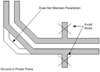 Figure 8-1 Differential Signal Pair - Stubs
Ideally, there must be no crossover or through on the signal paths. Vias present impedance discontinuities and must be minimized. Route an entire trace pair on a single layer if possible. PCB trace lengths must be kept as short as possible.
Signal traces must not be run such that they cross a plane split. See Figure 8-2. A signal crossing a plane split may cause unpredictable return path currents and would likely impact signal quality as well, potentially creating EMI problems.
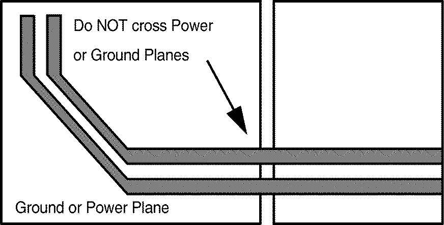 Figure 8-2 Differential Signal Pair-Plane Crossing
MDI signal traces must have 50 Ω to ground or 100-Ω differential controlled impedance. Many tools are available online to calculate this.
8.1.1 PCB Layer Stacking
To meet signal integrity and performance requirements, at minimum a 4-layer PCB is recommended for implementing PHYTER components in end user systems. The following layer stack-ups are recommended for four, six, and eight-layer boards, although other options are possible.
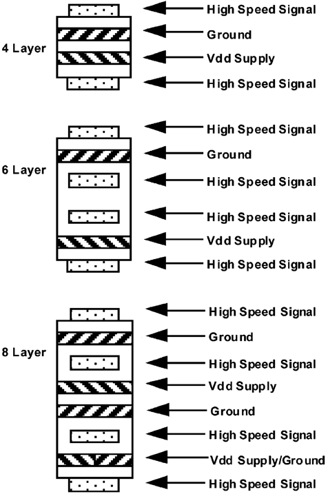 Figure 8-3 PCB Stripline Layer Stacking
Within a PCB it may be desirable to run traces using different methods, microstrip vs. stripline, depending on the location of the signal on the PCB. For example, it may be desirable to change layer stacking where an isolated chassis ground plane is used. Figure 8-4 illustrates alternative PCB stacking options.
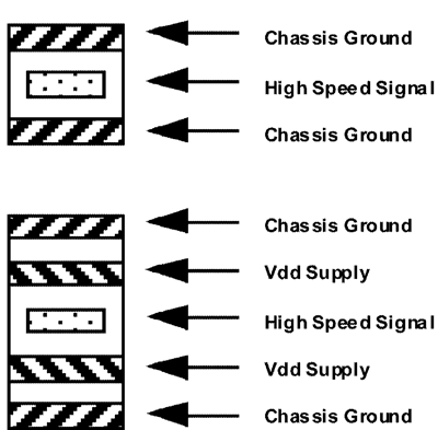 Figure 8-4 Alternative PCB Stripline Layer Stacking
8.2 Layout Example
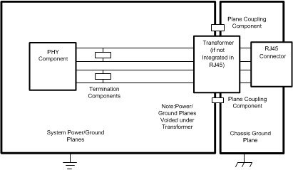 Figure 8-5 Layout Example