SNLS250E May   2008  – April 2015 DP83848H , DP83848J , DP83848K , DP83848M , DP83848T

PRODUCTION DATA.  

  1. 1Device Overview
    1. 1.1 Features
    2. 1.2 Applications
    3. 1.3 Description
    4. 1.4 Functional Block Diagram
  2. 2Revision History
  3. 3 Device Comparison
  4. 4Pin Configuration and Functions
    1. 4.1  Pin Diagram
    2. 4.2  Package Pin Assignments
    3. 4.3  Serial Management Interface
    4. 4.4  Mac Data Interface
    5. 4.5  Clock Interface
    6. 4.6  LED Interface
    7. 4.7  Reset
    8. 4.8  Strap Options
    9. 4.9  10 Mb/s and 100 Mb/s PMD Interface
    10. 4.10 Special Connections
    11. 4.11 Power Supply Pins
  5. 5Specifications
    1. 5.1 Absolute Maximum Ratings
    2. 5.2 ESD Ratings
    3. 5.3 Recommended Operating Conditions
    4. 5.4 Thermal Information
    5. 5.5 DC Specifications
    6. 5.6 AC Timing Requirements
  6. 6Detailed Description
    1. 6.1 Overview
    2. 6.2 Functional Block Diagram
    3. 6.3 Feature Description
      1. 6.3.1 Auto-Negotiation
        1. 6.3.1.1 Auto-Negotiation Pin Control
        2. 6.3.1.2 Auto-Negotiation Register Control
        3. 6.3.1.3 Auto-Negotiation Parallel Detection
        4. 6.3.1.4 Auto-Negotiaion Restart
        5. 6.3.1.5 Auto-Negotiation Complete Time
      2. 6.3.2 Auto-MDIX
      3. 6.3.3 LED Interface
        1. 6.3.3.1 LED
        2. 6.3.3.2 LED Direct Control
      4. 6.3.4 Internal Loopback
      5. 6.3.5 BIST
      6. 6.3.6 Energy Detect Mode
    4. 6.4 Device Functional Modes
      1. 6.4.1 MII Interface
        1. 6.4.1.1 Nibble-wide MII Data Interface
        2. 6.4.1.2 Collision Detect
        3. 6.4.1.3 Carrier Sense
      2. 6.4.2 Reduced MII Interface
      3. 6.4.3 802.3 MII Serial Management Interface
        1. 6.4.3.1 Serial Management Register Access
        2. 6.4.3.2 Serial Management Access Protocol
        3. 6.4.3.3 Serial Management Preamble Suppression
      4. 6.4.4 PHY Address
        1. 6.4.4.1 MII Isolate Mode
      5. 6.4.5 Half Duplex vs Full Duplex
      6. 6.4.6 Reset Operation
        1. 6.4.6.1 Hardware Reset
        2. 6.4.6.2 Software Reset
      7. 6.4.7 Power Down
    5. 6.5 Programming
      1. 6.5.1 Architecture
        1. 6.5.1.1 100BASE-TX Transmitter
          1. 6.5.1.1.1 Code-Group Encoding and Injection
          2. 6.5.1.1.2 Scrambler
          3. 6.5.1.1.3 NRZ to NRZI Encoder
          4. 6.5.1.1.4 Binary to MLT-3 Convertor
        2. 6.5.1.2 100BASE-TX Receiver
          1. 6.5.1.2.1  Analog Front End
          2. 6.5.1.2.2  Digital Signal Processor
          3. 6.5.1.2.3  Digital Adaptive Equalization and Gain Control
          4. 6.5.1.2.4  Base Line Wander Compensation
          5. 6.5.1.2.5  Signal Detect
          6. 6.5.1.2.6  MLT-3 to NRZI Decoder
          7. 6.5.1.2.7  NRZI to NRZ
          8. 6.5.1.2.8  Serial to Parallel
          9. 6.5.1.2.9  Descrambler
          10. 6.5.1.2.10 Code-Group Alignment
          11. 6.5.1.2.11 4B/5B Decoder
          12. 6.5.1.2.12 100BASE-TX Link Integrity Monitor
          13. 6.5.1.2.13 Bad SSD Detection
        3. 6.5.1.3 10BASE-T Transceiver Module
          1. 6.5.1.3.1  Operational Modes
          2. 6.5.1.3.2  Smart Squelch
          3. 6.5.1.3.3  Collision Detection and SQE
          4. 6.5.1.3.4  Carrier Sense
          5. 6.5.1.3.5  Normal Link Pulse Detection/Generation
          6. 6.5.1.3.6  Jabber Function
          7. 6.5.1.3.7  Automatic Link Polarity Detection and Correction
          8. 6.5.1.3.8  Transmit and Receive Filtering
          9. 6.5.1.3.9  Transmitter
          10. 6.5.1.3.10 Receiver
    6. 6.6 Memory
      1. 6.6.1 Register Block
        1. 6.6.1.1 Register Definition
          1. 6.6.1.1.1 Basic Mode Control Register (BMCR)
          2. 6.6.1.1.2 Basic Mode Status Register (BMSR)
          3. 6.6.1.1.3 PHY Identifier Register #1 (PHYIDR1)
          4. 6.6.1.1.4 PHY Identifier Register #2 (PHYIDR2)
          5. 6.6.1.1.5 Auto-Negotiation Advertisement Register (ANAR)
          6. 6.6.1.1.6 Auto-Negotiation Link Partner Ability Register (ANLPAR) (BASE Page)
          7. 6.6.1.1.7 Auto-Negotiation Link Partner Ability Register (ANLPAR) (Next Page)
          8. 6.6.1.1.8 Auto-Negotiate Expansion Register (ANER)
          9. 6.6.1.1.9 Auto-Negotiation Next Page Transmit Register (ANNPTR)
        2. 6.6.1.2 Extended Registers
          1. 6.6.1.2.1  PHY Status Register (PHYSTS)
          2. 6.6.1.2.2  False Carrier Sense Counter Register (FCSCR)
          3. 6.6.1.2.3  Receiver Error Counter Register (RECR)
          4. 6.6.1.2.4  100 Mb/s PCS Configuration and Status Register (PCSR)
          5. 6.6.1.2.5  RMII and Bypass Register (RBR)
          6. 6.6.1.2.6  LED Direct Control Register (LEDCR)
          7. 6.6.1.2.7  PHY Control Register (PHYCR)
          8. 6.6.1.2.8  10BASE-T Status/Control Register (10BTSCR)
          9. 6.6.1.2.9  CD Test and BIST Extensions Register (CDCTRL1)
          10. 6.6.1.2.10 Energy Detect Control (EDCR)
  7. 7Application, Implementation, and Layout
    1. 7.1 Application Information
    2. 7.2 Typical Application
      1. 7.2.1 Design Requirements
        1. 7.2.1.1 TPI Network Circuit
        2. 7.2.1.2 Clock IN (X1) Recommendations
          1. 7.2.1.2.1 Oscillator
          2. 7.2.1.2.2 Crystal
        3. 7.2.1.3 Power Feedback Circuit
        4. 7.2.1.4 Magnetics
      2. 7.2.2 Detailed Design Procedure
        1. 7.2.2.1 MAC Interface (MII/RMII)
          1. 7.2.2.1.1 Termination Requirement
          2. 7.2.2.1.2 Recommended Maximum Trace Length
        2. 7.2.2.2 Calculating Impedance
          1. 7.2.2.2.1 Microstrip Impedance - Single-Ended
          2. 7.2.2.2.2 Stripline Impedance - Single-Ended
          3. 7.2.2.2.3 Microstrip Impedance - Differential
          4. 7.2.2.2.4 Stripline Impedance - Differential
      3. 7.2.3 Application Curves
    3. 7.3 Layout
      1. 7.3.1 Layout Guidelines
        1. 7.3.1.1 PCB Layer Stacking
      2. 7.3.2 Layout Example
    4. 7.4 Power Supply Recommendations
  8. 8Device and Documentation Support
    1. 8.1 Documentation Support
      1. 8.1.1 Related Documentation
    2. 8.2 Related Links
    3. 8.3 Trademarks
    4. 8.4 Electrostatic Discharge Caution
    5. 8.5 Glossary
  9. 9Mechanical Packaging and Orderable Information

封装选项

机械数据 (封装 | 引脚)
散热焊盘机械数据 (封装 | 引脚)
订购信息

Mechanical Packaging and Orderable Information

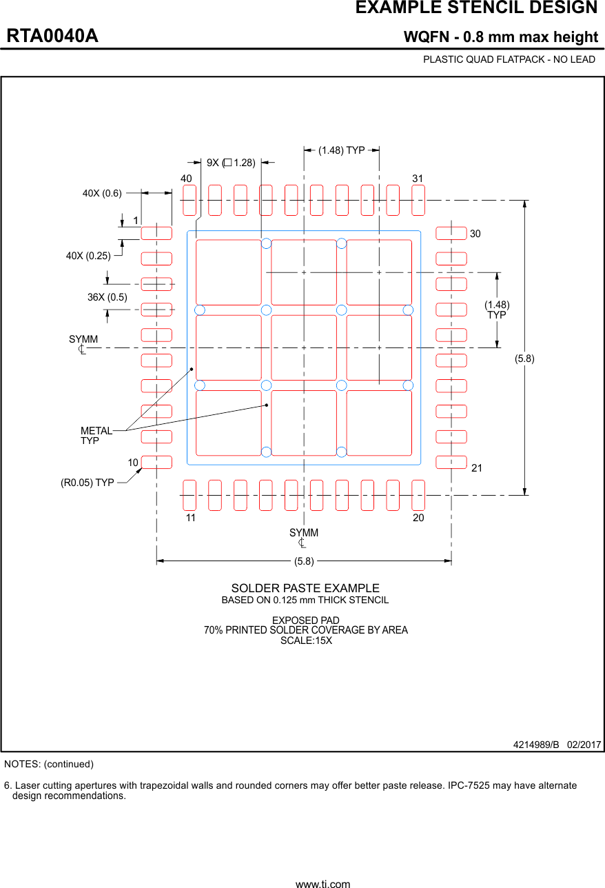
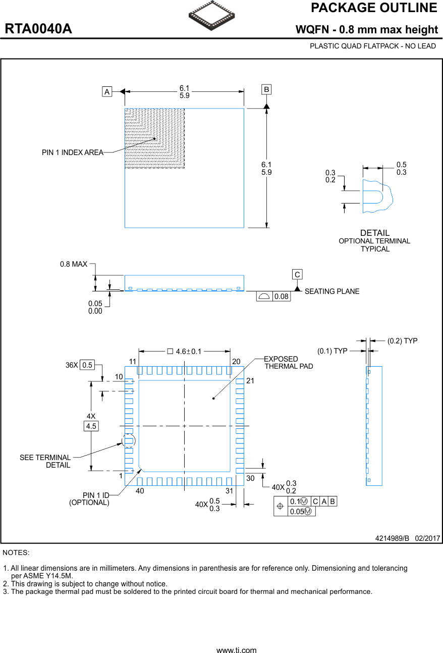
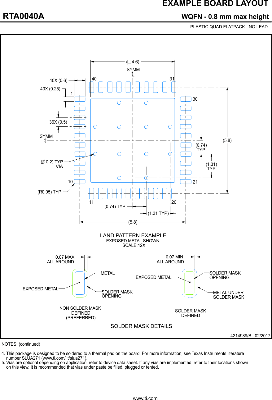
The following pages include mechanical, packaging, and orderable information. This information is the most current data available for the designated devices. This data is subject to change without notice and revision of this document. For browser-based versions of this data sheet, refer to the left-hand navigation.
DP83848H DP83848J DP83848K DP83848M DP83848T RTA0040A_4214989_Page_01.gif
DP83848H DP83848J DP83848K DP83848M DP83848T RTA0040A_4214989_Page_02.gif
DP83848H DP83848J DP83848K DP83848M DP83848T RTA0040A_4214989_Page_03.gif