ZHCSD09B September 2014 – October 2015 DLPA2005
PRODUCTION DATA.
- 1 特性
- 2 应用
- 3 说明
- 4 修订历史记录
- 5 Pin Configuration and Functions
- 6 Specifications
-
7 Detailed Description
- 7.1 Overview
- 7.2 Functional Block Diagram
- 7.3
Feature Description
- 7.3.1 DMD Regulators
- 7.3.2 RGB Strobe Decoder
- 7.3.3 LED Current Control
- 7.3.4 Maximum Led Currents and Efficiency Considerations
- 7.3.5 Calculating Inductor Peak Current
- 7.3.6 LED Current Accuracy
- 7.3.7 Transient Current Limiting
- 7.3.8 1.1-V Regulator (Buck Converter)
- 7.3.9 Measurement System
- 7.3.10
Protection Circuits
- 7.3.10.1 Thermal Warning (HOT) and Thermal Shutdown (TSD)
- 7.3.10.2 Low Battery Warning (BAT_LOW) and Undervoltage Lockout (UVLO)
- 7.3.10.3 DMD Regulator Fault (DMD_FLT)
- 7.3.10.4 V6V Power-Good (V6V_PGF) Fault
- 7.3.10.5 VLED Overvoltage (VLED_OVP) Fault
- 7.3.10.6 VLED Power Save Mode
- 7.3.10.7 V1V8 PG Failure
- 7.3.10.8 Interrupt Pin (INTZ)
- 7.3.10.9 SPI
- 7.3.11 Password Protected Registers
- 7.4 Device Functional Modes
- 7.5 Register Maps
- 8 Application and Implementation
- 9 Power Supply Recommendations
- 10Layout
- 11器件和文档支持
- 12机械、封装和可订购信息
7 Detailed Description
7.1 Overview
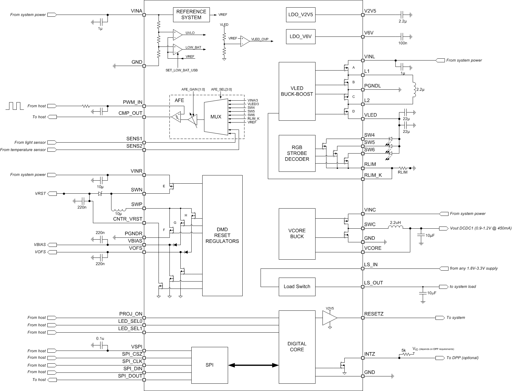
The DLPA2005 is a power management and LED driver IC optimized for DLP video and data display systems. DLPA2005 is part of the chipset comprising of either DLP2010 (.2WVGA) DMD and DLPC3430/DLPC3435 controller, the DLP2010NIR (.2WVGA-NIR) DMD and DLPC150 controller, or the DLP3010 (.3 720p) DMD and DLPC3433/DLPC3438 controller. The DLPA2005 contains a complete LED driver including high efficiency power convertors. The DLPA2005 can supply up to 2.4 A per LED. Integrated high-current switches are included for sequentially selecting R, G, and B LEDs. The DLPA2005 also contains three regulated DC supplies for the DMD reset circuitry: VBIAS, VRST and VOFS, as well as a regulated DC supply of 1.1 V and a load switch for the 1.8 V to support the controllers. The DLPA2005 has a SPI used for setting the configuration. Using SPI, currents can be set independently for each LED with 10-bit resolution. Other features included are the generation of the system reset, power sequencing, input signals for sequentially selecting the active LED, IC self-protections, and an analog MUX for routing analog information to an external ADC.
7.2 Functional Block Diagram
7.3 Feature Description
7.3.1 DMD Regulators
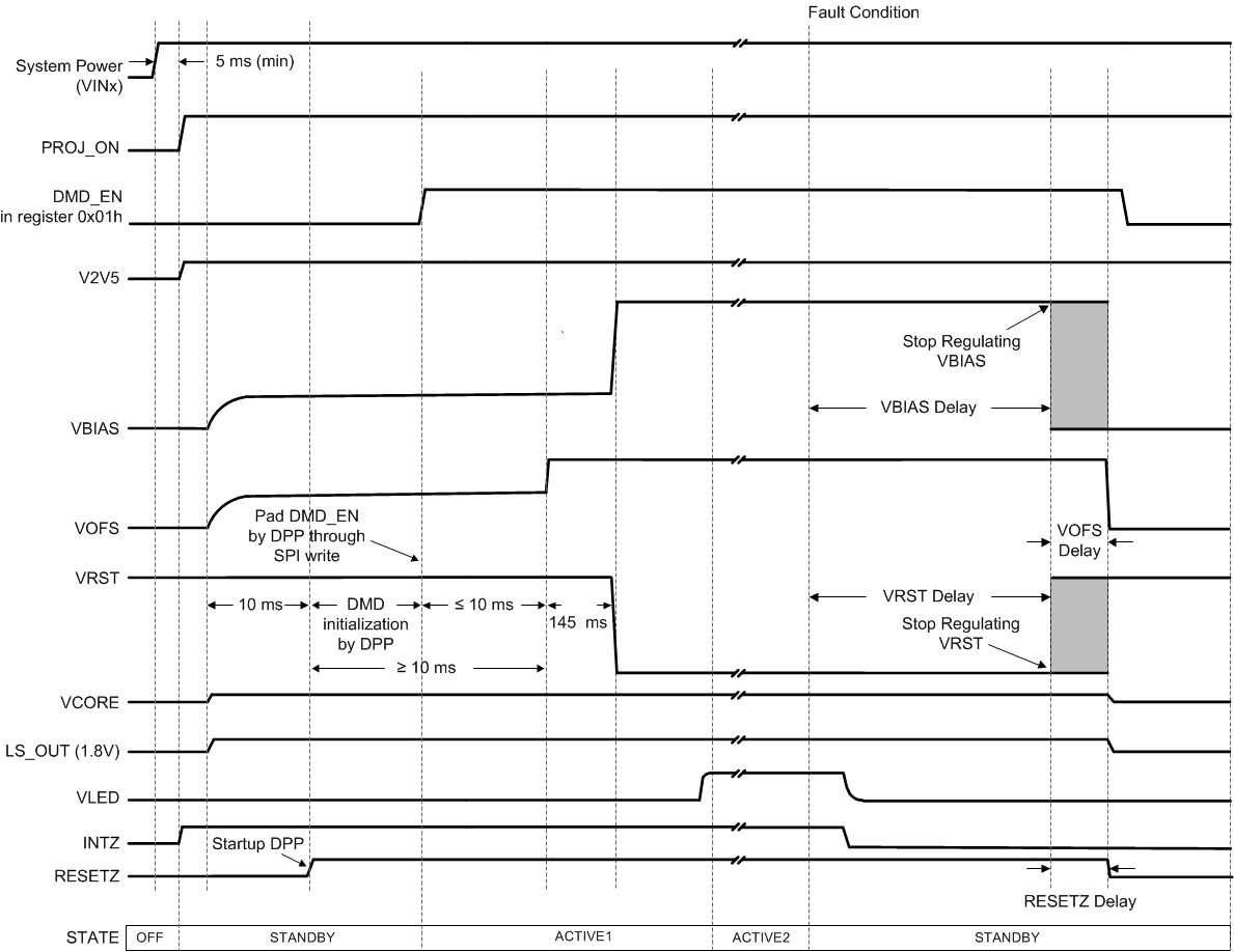
DLPA2005 contains three switch-mode power supplies that power the DMD. These rails are VOFS, VBIAS, and VRST. After pulling the PROJ_ON pin high, the DMD is first initialized followed by a power-up of the VOFS line after a small delay of less than 10 ms followed by VBIAS and VRST with an additional delay of 145 ms. The LED driver and STROBE DECODER circuit can only be enabled after all three rails are enabled. There are two power-down sequences, the normal power-down timing initiated after pulling the PROJ_ON pin low, and a fast power-down mode where if any one of the rails encounters a fault such as an output short, all three rails are discharged simultaneously. The detailed power-up and power-down diagrams are shown in Figure 3 and Figure 4.
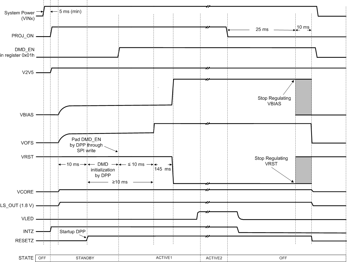 Figure 3. Power Sequence Normal Shutdown Mode
NOTE
All values are typical (unless otherwise noted).
NOTE
All values are typical (unless otherwise noted).
7.3.2 RGB Strobe Decoder
DLPA2005 contains RGB color-sequential circuitry that is composed of three NMOS switches, the LED driver, the strobe decoder, and the LED current control. The NMOS switches are connected to the terminals of the external LED package and turn the currents through the LEDs on and off. Package connections are shown in Figure 5 and Figure 9 and corresponding switch map in Table 1.
The LED_SEL[1:0] signals typically receive a rotating code switching from RED to GREEN to BLUE and then back to RED. When the LED_SEL[1:0] input signals select a specific color, the NMOSFETs are controlled based on the color selected, and a 10-bit current control DAC for this color is selected that provides a control current to the RGB LEDs feedback control network.
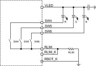 Figure 5. Switch Connection for a Common-Anode LED Assembly
Table 1. Switch Positions for Common Anode RGB LEDs (MAP = 0)
| Common Anode | ||||
|---|---|---|---|---|
| LED_SEL[1:0] | SW6 | SW5 | SW4 | IDAC Input |
| 0x00h | Open | Open | Open | N/A |
| 0x01h | Open | Open | Closed | SW4_IDAC[9:0] |
| 0x02h | Open | Closed | Open | SW5_IDAC[9:0] |
| 0x03h | Closed | Open | Open | SW6_IDAC[9:0] |
The switching of the three NMOS switches is controlled such that switches are returned to the open position first before the closed connections are made (break before make). The dead time between opening and closing switches is controlled through the BBM register. Switches that already are in the closed position (and are to remain in the closed state according to the SWCNTRL register) are not opened during the BBM delay time.
 Figure 6. BBM Timing (See Register 0Bh in Table 19)
7.3.3 LED Current Control
DLPA2005 provides time-sequential circuitry to drive three LEDs with independent current control. A system based on a common anode LED configuration is shown in Figure 9 and consists of a buck-boost converter, which provides the voltage to drive the LEDs, three switches connected to the cathodes of the LEDs, an RLIM resistor used to sense the LED current, and a current DAC to control the LED current. The voltage measured at the pin V(RLIM_K) is used by the regulator loop.
The STROBE DECODER controls the switch positions as described in the previous section (RGB Strobe Decoder ). With all switches in the open position, the buck-boost output assumes an output voltage of 3.5 V.
For a common-anode RGB LED configuration, the buck-boost output voltage (VLED) assumes a value such that the voltage drop across the sense resistor equals
SPACE
SPACE
when SW4 is closed. The exact value of VLED depends on the current setting and the voltage drop across the LED but is limited to 5.4 V. When the STROBE decoder switches from SW4 to SW5, the buck-boost assumes a new output voltage such that the sense voltage equals:
SPACE
SPACE
and finally when SW6 is selected.
SPACE
SPACE
7.3.4 Maximum Led Currents and Efficiency Considerations
The DLPA2005 comprises a buck-boost power converter to supply the appropriate VLED to the LEDs. The maximum obtainable LED current for a given LED forward voltage are limited by three items:
- The inherent maximum LED current of the PAD2005, i.e. for DAC setting 03FFh.
- The maximum input current of about 4 A.
- The converter efficiency.
- Junction and ambient temperature
In the Figure 2 graph the LED current versus DAC setting is given for several supply voltages (VIN). The load was configured for each supply case such that at the maximum attainable current VOUT max=4.8 V.
For the higher supply voltages VIN>4.5 V the DAC current increases linearly up to the max setting of 3FFh. At that setting the ILED is about 2.5 A. For VIN=2.3 V and VIN=2.7 V the LED current is typically limited to 0.9 A and 1.3 A, respectively. Main reason of this limitation is the maximum input current in combination with the limited converter efficiency. This can be understood by looking at the equation describing the power conversion:
SPACE

| This equation states that the output power of the converter is equal to the input power times the converter efficiency. As indicated above, the input current IIN of the power converter is maximized to about 4A. The neff is the efficiency of the power converter, as described further down this section. For the lower input voltage the power converter runs as a boost converter. | ||
| (VOUT=4.8 V). Assuming 100% efficiency, VIN=2.3 V, VOUT=4.8 V and IINmax=4 A, the maximum attainable ILED is: |
For the power converter approaching the maximum input current, the efficiency can roll down significantly. As a result the maximum LED current for VIN=2.3 V and VOUT=4.8 V is about 0.9 A.
The efficiency of the power converter depends on the input supply voltage and the output loading, i.e. output voltage and output current. In the below graph efficiency curves as a function of the LED current are given for several input supply voltages. Again for each of these supply cases the load was controlled such that at maximum output current the output voltage was about 4.8 V.
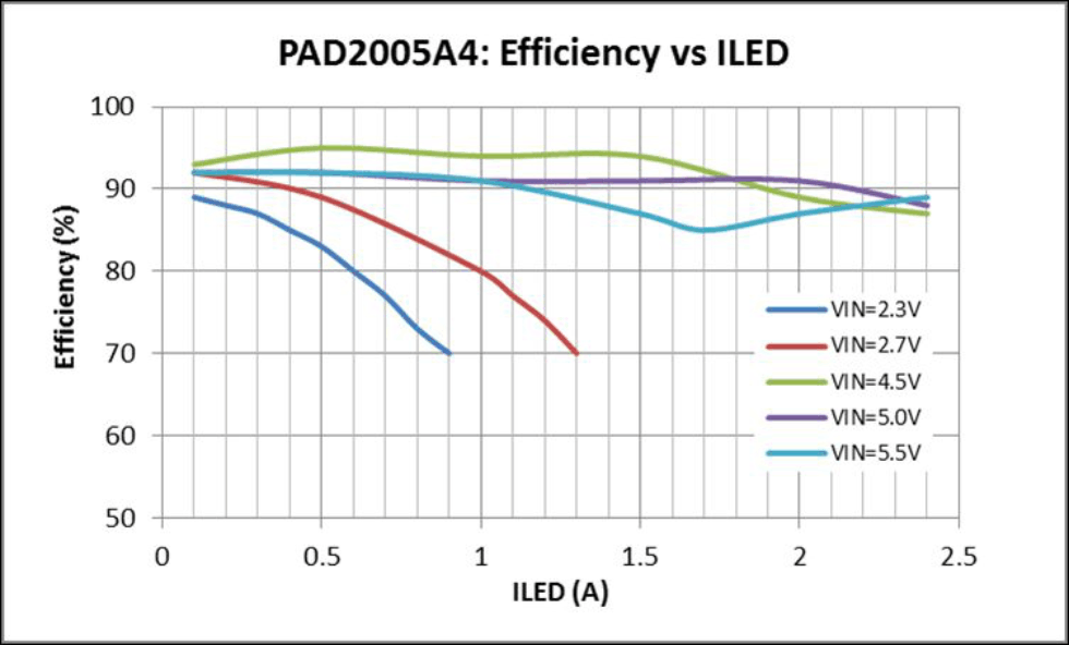 Figure 7. Measured Typical Power converter efficiency as a function of ILED for several supply voltages (VOUTmax=4.8V for each supply)
Note that in the measurement the output of the buck-boost regulator includes the voltage drop across the sense resistor RLIM, the voltage drop across the internal strobe control switch, and the forward voltage of the LED.
For higher input voltages the power converter runs at an efficiency of 85% or better. For the lower supply voltages because of the boost action, the efficiency quickly rolls down. Refer to section Thermal Considerations for information related to these efficiencies.
7.3.5 Calculating Inductor Peak Current
To properly configure the DLPA2005 device, a 2.2-μH inductor must be connected between pin L1 and pin L2. The peak current for the inductor in steady state operation can be calculated.
Equation 4 shows how to calculate the peak current I1 in step down mode operation, and Equation 5 shows how to calculate the peak current I2 in boost mode operation. VIN1 is the maximum input voltage, VIN2 is the minimum input voltage, ƒ is the switching frequency (2.25 MHz), and L the inductor value (2.2 μH).


The critical current value for selecting the right inductor is the higher value of I1 and I2. Also consider that load transients and error conditions may cause higher inductor currents. This needs to be accounted for when selecting an appropriate inductor. Internally the switching current is limited to a maximum of 4 A.
7.3.6 LED Current Accuracy
The LED drive current is controlled by a current DAC (Digital to Analog Converter) and can be set independently for switch SW4, SW5 and SW6. For the DLPA2005, the DAC is trimmed at a current of 2528 mA at code: 0x3FFh, and the step size is 2.47 mA. First order gain-error of the DAC can be neglected, but an offset current error must be taken into account. This offset error differs depending on the used RLIM, and is ±100 mA for the DLPA2005 using a current sense resistor of 39 mΩ.
The max current of the DLPA2005 (SWx_IDAC[9:0] = 0x3FFh) is regulated to 2528 mA. At the lowest setting (SWx_IDAC[9:0] = 0x029h) the current is regulated to 101 mA (DLPA2005). For this current setting (0x028h), the absolute current error results into a large relative error, however this is not a typical operating point.
For best accuracy of the LED current, take the below two considerations into account:
- The LED current setting does not only depend on the accuracy of the RLIM resistor but also strongly depends on the added resistance of pcb traces in the ground route of RLIM and the soldering quality. Due to the low value of the current sense resistor RLIM, any extra introduced resistance of e.g. several milliohms will result in a noticeable different LED current.
- Voltage sensing across RLIM is internally referred to the analog ground, i.e. pin 5 AGND1 and pin 20 GND. To prevent any voltage drop between the ground connection of RLIM and the AGND of the PAD2005, make a star connection of the RLIM ground near pin 5. Take care to make it a low ohmic route that can handle the high LED current. Subsequently, make the ground connection for pin 5 to the system ground low ohmic as well.
Taking the above measures relative to RLIM, the ILED current should align with the calculated value according to:
- Decimal_Code# = (set_current - min_current)/ step_current.
- If needed translate the Decimal_Code# to HEX code before entering in the control software.
7.3.7 Transient Current Limiting
Typically the forward voltages of the green and blue diodes are close to each other (about 3 to 4 V). However, the forward voltage of the red diode is significantly lower (1.8 to 2.5 V). This can lead to a current spike in the red diode when the strobe controller switches from green or blue to red because VLED is initially at a higher voltage than required to drive the RED diode. DLPA2005 provides transient current limiting for each switch to limit the current in the LEDs during the transition. The transient current limit value is controlled through the ILIM[3:0] bits in the IREG register. The same register also contains three bits to select which switch employs the transient current limiting feature. In a typical application, the transient current limit will only apply to the RED diode, and the ILIM[3:0] value will typically be set approximately 10% higher than the DC regulation current. The effect that the transient current limit has on the LED current is shown in Figure 8.
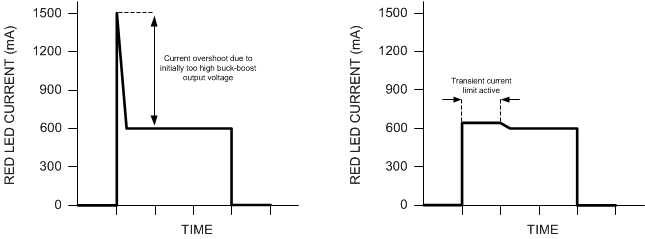
| Red LED current without transient current limit. The current overshoots because the buck-boost voltage starts at the (higher) level of the green or blue LED. | LED current with transient current limit. | |
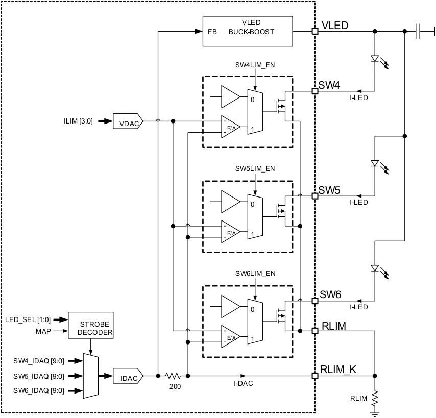 Figure 9. LED Driver Block Diagram
7.3.8 1.1-V Regulator (Buck Converter)
The buck converter creates a voltage of 1.1 V, and due to its switching nature, an output ripple with a frequency of approximately 2.25 MHz occurs on its output. This ripple is strongly dependent on the decoupling capacitor at the output in combination with the inductor. The magnitude of the ripple can be calculated with Equation 6.

The best way to minimize this ripple is to select a capacitor with a very-low ESR.
7.3.9 Measurement System
The measurement system is composed of a 10:1 analog multiplexer (MUX), a programmable-gain amplifier, and a comparator. It works together with the DPP processor to provide:
- White-point correction (WPC) by independently adjusting the RGB LED currents after measuring the brightness of each color with an external light sensor
- A measurement of the:
- Battery voltage
- LED forward voltage
- Exact LED current
- Temperature as derived by measuring the voltage across an external thermistor
Figure 10 shows a block diagram of the measurement system.
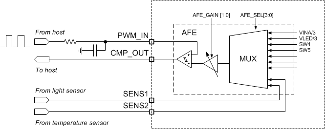 Figure 10. Block Diagram of the Measurement System
Table 2. Recommended Configuration of the AFE for Different Input Selections
| AFE_SEL[3:0] | SELECTED INPUT | RECOMMENDED GAIN SETTING AFE-GAIN[1:0] |
RECOMMENDED SETTING OF AFE_CAL_DIS BIT |
|---|---|---|---|
| 0x00h | SENS2 | 0x01h (1x) | Setting has no effect on measurement |
| 0x01h | VLED | 0x01h (1x) | Setting has no effect on measurement |
| 0x02h | VINA | 0x01h (1x) | Setting has no effect on measurement |
| 0x03h | SENS1 | 0x01h (1x) | Setting has no effect on measurement |
| 0x04h | RLIM_K | 0x03h (18x) | Set to 1 if sense voltage is >100 mV. Otherwise set to 0 (default) |
| 0x05h | SW4 | 0x02h (9.5x) | Set to 1 if sense voltage is >200 mV. Otherwise set to 0 (default) |
| 0x06h | SW5 | 0x02h (9.5x) | Set to 1 if sense voltage is >200 mV. Otherwise set to 0 (default) |
| 0x07h | SW6 | 0x02h (9.5x) | Set to 1 if sense voltage is >200 mV. Otherwise set to 0 (default) |
| 0x08h | No connect | N/A | N/A |
| 0x09h | VREF | 0x01h (1x) | Setting has no effect on measurement |
7.3.10 Protection Circuits
DLPA2005 has several protection circuits to protect the IC and system from damage due to excessive power consumption, die temperature, or over-voltages. These circuits are described in the following sections.
7.3.10.1 Thermal Warning (HOT) and Thermal Shutdown (TSD)
DLPA2005 continuously monitors the junction temperature and issues a HOT interrupt if temperature exceeds the HOT threshold. If the temperature continues to increase above the thermal shutdown threshold, all rails are disabled and the TSD bit in the INT register is set. After the temperature drops below its threshold, the system recovers and waits for the DPP to resend the DMD_EN bit.
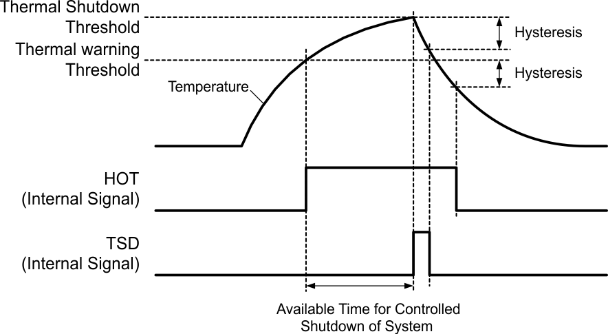 Figure 11. Definition of the Thermal Shutdown and Hot-Die Temperature Warning
7.3.10.2 Low Battery Warning (BAT_LOW) and Undervoltage Lockout (UVLO)
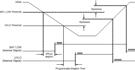
If the battery voltage drops below the BAT_LOW threshold (typically 3 V) the BAT_LOW interrupt is issued, but normal operation continues. After the battery drops below the undervoltage threshold which has a default hardcoded value of 2.3 V (this UVLO voltage can be changed through register 09 h from 2.3 to 4.5 V), the UVLO interrupt is issued, all rails are powered down in sequence, the DMD_EN bit is reset, and the part enters STANDBY mode. The power rails cannot be re-enabled before the input voltage recovers to >2.4 V. To re-enable the rails, the PROJ_ON pin must be toggled. The undervoltage threshold is programmable from 2.3 to 4.5 V in 31 steps.
The UVLO shutdown process will protect the DMD by allowing time for the mirrors to park, then doing a fast discharge of VOFS, VRST, and VBIAS. This protection occurs even in the case of sudden battery removal from the projector, as long as the bulk capacitance on the battery voltage (VINx) keeps this voltage above 2.3 V for as long as needed for VOFS, VRST, and VBIAS to discharge to the required safe levels as shown in the DMD data sheet. VOFS, VRST, and VBIAS discharge times depend on the load capacitance on each regulator. When for instance every supply is decoupled using a capacitor of 0.5 µF, VINx should stay above 2.3 V for at least 100 µs after the battery is suddenly removed. During this time, the mirrors can be placed in a safe position and VOFS, VRST, and VBIAS can be discharged.
NOTE
Capacitive loads should be such that LS_OUT stays above 1.65 V until VOFS, VRST, and VBIAS have discharged to their required safe levels.
7.3.10.3 DMD Regulator Fault (DMD_FLT)
The DMD regulator is continuously monitored to check if the output rails are in regulation and if the inductor current increases as expected during a switching cycle. If either one of the output rails drops out of regulation (for example, due to a shorted output) or the inductor current does not increase as expected during a switching cycle (due to a disconnected inductor), the DMD_FLT interrupt bit is set in the INT register, the DMD_EN bit is reset, and the DMD regulator is shut down. Resetting the DMD_EN bit also causes the LED driver to power down. To restart the system, the PROJ_ON pin must be toggled. In case the interrupt is masked, it is sufficient to set the DMD_EN bit to restart the system.
7.3.10.4 V6V Power-Good (V6V_PGF) Fault
The LED driver regulation loop requires the V6V rail for proper operation. The rail is continuously monitored and should the output drop below the power-good threshold, the V6V_PGF bit is set. The VLED buck-boost is then disabled and attempts to restart automatically.
7.3.10.5 VLED Overvoltage (VLED_OVP) Fault
If the buck-boost output voltage rises above 5.4 V, the VLED_OVP interrupt is set but the buck-boost regulator is not turned off. A typical condition to cause this fault is an open LED.
7.3.10.6 VLED Power Save Mode
In normal PWM operation, the efficiency of the VLED buck-boost converter dramatically reduces for LED currents below 100 mA. In this case, the power save mode allows high converting efficiency at low output currents by skipping pulses in the switcher’s gate driver control.
7.3.10.7 V1V8 PG Failure
If for any reason the voltage on the LS_OUT drops below approximately 1.3 V, then VOFS, VBIAS, and VRST immediately go into fast shut down. Holding off power down to do mirror parking is not included since 1.3 V is too low to wait for this. Reactivating can only be done by toggling the PROJ_ON off and on again.
7.3.10.8 Interrupt Pin (INTZ)
Use the interrupt pin to signal events and fault conditions to the host processor. Whenever a fault or event occurs in the IC, the corresponding interrupt bit is set in the INT register, and the open-drain output is pulled low. The INTZ pin is released (returns to HiZ state) and fault bits are cleared when the INT register is read by the host.
However, if a failure persists, the corresponding INT bit remains set and the INTZ pin is pulled low again after a maximum of 32 µs.
Interrupt events include fault conditions such as power-good faults, over-voltage, over-temperature shutdown, and UVLO. For all interrupt conditions see the interrupt register on Table 21.
The MASK register is used to mask events from generating interrupts, that is, from pulling the INTZ pin low. The MASK settings affect the INTZ pin only and have no impact on protection and monitor circuits themselves. When an interrupt is masked, the event causing the interrupt still sets the corresponding bit in the INT register. However, it does not pull the INTZ pin low.
7.3.10.9 SPI
DLPA2005 provides a 4-wire SPI port that supports high-speed serial data transfers up to 33.3 MHz. Support includes register and data buffer write and read operations. The SPI_CSZ input serves as the active low chip select for the SPI port. The SPI_CSZ input must be forced low in order to write or read registers and data buffers. When SPI_CSZ is forced high, the data at the SPI_DIN input is ignored, and the SPI_DOUT output is forced to a high-impedance state. The SPI_DIN input serves as the serial data input for the port; the SPI_DOUT output serves as the serial data output. The SPI_CLK input serves as the serial data clock for both the input and output data. Data is latched at the SPI_DIN input on the rising edge of SPI_CLK, while data is clocked out of the SPI_DOUT output on the falling edge of SPI_CLK. Figure 13 illustrates the SPI port protocol. Byte 0 is referred to as the command byte, where the most significant bit is the write/not read bit. For the W/nR bit, a 1 indicates a write operation, while a 0 indicates a read operation. The remaining seven bits of the command byte are the register address targeted by the write or read operation. The SPI port supports write and read operations for multiple sequential register addresses through the implementation of an auto-increment mode. As shown in Figure 13, the auto-increment mode is invoked by simply holding the SPI_CSZ input low for multiple data bytes. The register address is automatically incremented after each data byte transferred, starting with the address specified by the command byte. After reaching address 0x7Fh the address pointer jumps back to 0x00h.
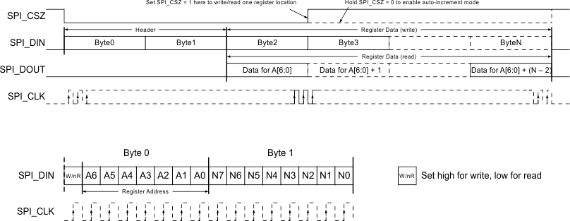 Figure 13. SPI Protocol
7.3.11 Password Protected Registers
Register addresses 0x11h through 0x27h can be read-accessed the same way as any other register, but are protected against accidental write operations through the PASSWORD register (address 0x10h). To write to a protected register, follow these steps:
- Write data 0xBAh to register address 0x10h.
- Write data 0xBEh to register address 0x10h.
Both writes must be consecutive, that is, there must be no other read or write operation in between sending the two bytes. After the password has been successfully written, registers 0x11h through 0x27h are unlocked and can be write accessed using the regular SPI protocol. They remain unlocked until any byte other than 0xBAh is written to the PASSWORD register or the part is power cycled.
To check if the registers are unlocked, read back the PASSWORD register. If the data returned is 0x00h, the registers are locked. If the PASSWORD register returns 0x01h, the registers are unlocked.
7.4 Device Functional Modes
MODES OF OPERATION
-
OFF This is the lowest-power mode of operation. All power functions are turned off, registers are reset to their default values and the IC does not respond to SPI commands. RESETZ pin is pulled low. The IC will enter OFF mode whenever the PROJ_ON pin is low.
-
STANDBY The DMD regulators and LED power (VLED) are turned off, but the IC does respond to the SPI interface. The device enters STANDBY mode whenever PROJ_ON is set high or DMD_EN7 bit is set to 0 using the SPI interface after PROJ_ON is already high. The device also enters STANDBY mode when a fault condition is detected8. (see the section about Protection Circuits on pages 28 & 30)
-
ACTIVE1 The DMD supplies are enabled but LED power (VLED) is disabled. PROJ_ON pin must be high, DMD_EN bit must be set to 1, and VLED_EN9 bit is set to 0.
-
ACTIVE2 DMD supplies and LED power are enabled. PROJ_ON pin must be high and DMD_EN and VLED_EN bits must both be set to 1.
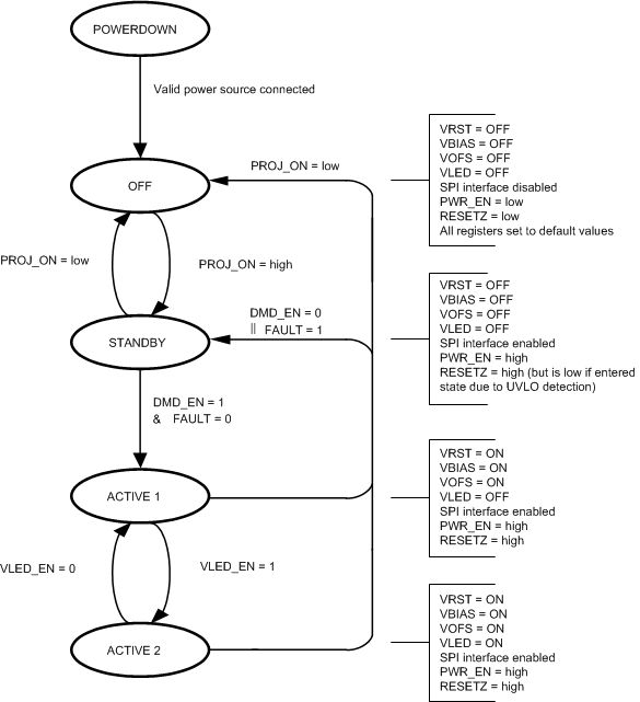
Table 3. Device State as a Function of Control-Pin Status
| PROJ_ON PIN | STATE |
|---|---|
| LOW | OFF |
| HIGH | STANDBY ACTIVE1 ACTIVE2 (Device state depends on DMD_EN and VLED_EN bits and whether there are any fault conditions.) |
Table 4. Modes of Operation
| MODE | DESCRIPTION |
|---|---|
| OFF | This is the lowest-power mode of operation. All power functions are turned off, registers are reset to their default values, and the IC does not respond to SPI commands. RESETZ pin is pulled low. The IC will enter OFF mode whenever the PROJ_ON pin is low. |
| STANDBY | The DMD regulators and LED power (VLED) are turned off, but the IC does respond to the SPI. The device enters STANDBY mode whenever PROJ_ON is set high or DMD_EN(1) bit is set to 0 using the SPI interface after PROJ_ON is already high. The device also enters STANDBY mode when a fault condition is detected(2). (See Protection Circuits .) |
| ACTIVE1 | The DMD supplies are enabled but LED power (VLED) is disabled. PROJ_ON pin must be high, DMD_EN bit must be set to 1, and VLED_EN(3) bit is set to 0. |
| ACTIVE2 | DMD supplies and LED power are enabled. PROJ_ON pin must be high and DMD_EN and VLED_EN bits must both be set to 1. |
7.5 Register Maps
Table 5. Register Description
| REGISTER | ADDRESS (Hex) | NAME | TABLE | DESCRIPTION | DEFAULT |
|---|---|---|---|---|---|
| USER CONFIGURATION DEFINITIONS | |||||
| R | 0x00 | CHIP ID | Table 6 | Chip Revision Register; DLPA2005 | C4 |
| R/W | 0x01 | CHIPENABLE | Table 7 | Enable Register | 0F |
| R/W | 0x02 | IREG | Table 1 | Transient-current limit settings | 30 |
| R/W | 0x03 | SW4MSB | Table 8 | Regulation current MSB, SW4 | 0 |
| R/W | 0x04 | SW4LSB | Table 9, Table 10 | Regulation current LSB, SW4 | 0 |
| R/W | 0x05 | SW5MSB | Table 11 | Regulation current MSB, SW5 | 0 |
| R/W | 0x06 | SW5LSB | Table 12, Table 13 | Regulation current LSB, SW5 | 0 |
| R/W | 0x07 | SW6MSB | Table 14 | Regulation current MSB, SW6 | 0 |
| R/W | 0x08 | SW6LSB | Table 15, Table 16 | Regulation current LSB, SW6 | 0 |
| R/W | 0x09 | SWCNTRL | Table 17 | Switch ON/OFF control (direct mode) | 0 |
| R/W | 0x0A | AFE | Table 18 | AFE (MUX) control | 0 |
| R/W | 0x0B | BBM | Table 19, Table 20 | Break Before Make timing | 0 |
| R | 0x0C | INT | Table 21, Table 22 | Interrupt register | 0 |
| R/W | 0x0D | INT MASK | Table 23, Table 24 | Interrupt Mask register | DFh |
| R/W | 0x0E | TIMING | Table 25, Table 26 | Timing register VOFS, VBIAS, VRST, and RESETZ | 7 |
| USER PROTECTED DEFINITION | |||||
| R/W | 0x10 | PASSWORD | Table 27 | Password register | 0 |
| R/W | 0x11 | SYSTEM | Table 28 | System Configuration register | 0 |
| USER EEPROM SCRATCH PAD DEFINITION | |||||
| R/W | 0x20 | BYTE0 | Table 30 | User EEPROM, Byte0 | 0 |
| R/W | 0x21 | BYTE1 | Table 31 | User EEPROM, Byte1 | 0 |
| R/W | 0x22 | BYTE2 | Table 32 | User EEPROM, Byte2 | 0 |
| R/W | 0x23 | BYTE3 | Table 33 | User EEPROM, Byte3 | 0 |
| R/W | 0x24 | BYTE4 | Table 34 | User EEPROM, Byte4 | 0 |
| R/W | 0x25 | BYTE5 | Table 35 | User EEPROM, Byte5 | 0 |
| R/W | 0x26 | BYTE6 | Table 36 | User EEPROM, Byte6 | 0 |
| R/W | 0x27 | BYTE7 | Table 37 | User EEPROM, Byte7 | 0 |
Table 6. Chip Revision Register
| REGISTER = 00h | |||||||||
|---|---|---|---|---|---|---|---|---|---|
| DATA BIT | D7 | D6 | D5 | D4 | D3 | D2 | D1 | D0 | HEX |
| FIELD NAME | CHIP ID [7:0] | ||||||||
| READ/WRITE | R | R | R | R | R | R | R | R | |
| RESET VALUE DLPA2005 | 1 | 1 | 0 | 0 | 0 | 1 | 0 | 0 | C4 |
| FIELD NAME | BIT | BIT DEFINITION | |||||||
| CHIP ID | [7:0] | 7:4 | CHIPID<3:0> | ||||||
| 3:0 | REVID<3:0> | ||||||||
Table 7. Enable Register
| REGISTER = 01h | |||||||||
|---|---|---|---|---|---|---|---|---|---|
| DATA BIT | D7 | D6 | D5 | D4 | D3 | D2 | D1 | D0 | HEX |
| FIELD NAME | CHIPENABLE [15:8] | ||||||||
| READ/WRITE | R/W | R/W | R/W | R/W | R/W | R/W | R/W | R/W | |
| RESET VALUE | 0 | 0 | 0 | 0 | 1 | 1 | 1 | 1 | 0F |
| FIELD NAME | BIT | BIT DEFINITION | |||||||
| CHIPENABLE | [15:8] | 15:12 | USER_GPO<3:0> | ||||||
| 11 | VLED_POWER_SAVE_MODE_DIS Power save mode is used to improve efficiency at light load. |
||||||||
| 10 | FAST_SHUTDOWN_EN Applicable only during a fault condition. Shutdown timing is defined by register 0Eh. (see Figure 5) |
||||||||
| 9 | DMD_EN | ||||||||
| 8 | VLED_EN | ||||||||
Table 1. Transient-Current Limit Settings
| REGISTER = 02h | |||||||||
| DATA BIT | D7 | D6 | D5 | D4 | D3 | D2 | D1 | D0 | HEX |
| Field Name | IREG [23:16] | ||||||||
| Read/Write | R/W | R/W | R/W | R/W | R/W | R/W | R/W | R/W | |
| Reset Value | 0 | 0 | 1 | 1 | 0 | 0 | 0 | 0 | 30 |
| FIELD NAME | BIT | BIT DEFINITION | |||||||
| Not used | [23:16] | 23 | TBD | ||||||
| IREG [3:0] | 22:19 | IREG_ILIM<3:0> | Rlim = 39 mΩ | ||||||
| 0000 | 333 mA | ||||||||
| 0001 | 385 mA | ||||||||
| 0010 | 442 mA | ||||||||
| 0011 | 494 mA | ||||||||
| 0100 | 564 mA | ||||||||
| 0101 | 705 mA | ||||||||
| 0110 | 846 mA | ||||||||
| 0111 | 1128 mA | ||||||||
| 1000 | 1410 mA | ||||||||
| 1001 | 1692 mA | ||||||||
| 1010 | 1974 mA | ||||||||
| 1011 | 2256 mA | ||||||||
| 1100 | 2538 mA | ||||||||
| 1101 | 2974 mA | ||||||||
| 1110 | 3410 mA | ||||||||
| 1111 | 3846 mA | ||||||||
| SW6LIM_EN | 18 | SW6LIM_EN | |||||||
| Transient current-limit enable for SW6 0 – Transient current-limit is disabled 1 – Transient current-limit is enabled |
|||||||||
| SW5LIM_EN | 17 | SW5LIM_EN | |||||||
| Transient current-limit enable for SW5 0 – Transient current-limit is disabled 1 – Transient current-limit is enabled |
|||||||||
| SW4LIM_EN | 16 | SW4LIM_EN | |||||||
| Transient current-limit enable for SW4 0 – Transient current-limit is disabled 1 – Transient current-limit is enabled |
|||||||||
Table 8. Regulation Current MSB, SW4(1)
| REGISTER = 03h | |||||||||
|---|---|---|---|---|---|---|---|---|---|
| DATA BIT | D7 | D6 | D5 | D4 | D3 | D2 | D1 | D0 | HEX |
| FIELD NAME | SW4MSB [31:24] | ||||||||
| READ/WRITE | R/W | R/W | R/W | R/W | R/W | R/W | R/W | R/W | |
| RESET VALUE | 0 | 0 | 0 | 0 | 0 | 0 | 0 | 0 | 00 |
| FIELD NAME | Bit | BIT DEFINITION | |||||||
| SW4MSB | [31:24] | 31:26 | TBD | ||||||
| 25:24 | SW4_IDAC<9:8> | ||||||||
Table 9. Regulation Current LSB, SW4
| REGISTER = 04h | |||||||||
|---|---|---|---|---|---|---|---|---|---|
| DATA BIT | D7 | D6 | D5 | D4 | D3 | D2 | D1 | D0 | HEX |
| FIELD NAME | SW4LSB [39:32] | ||||||||
| READ/WRITE | R/W | R/W | R/W | R/W | R/W | R/W | R/W | R/W | |
| RESET VALUE | 0 | 0 | 0 | 0 | 0 | 0 | 0 | 0 | 00 |
| FIELD NAME | Bit | BIT DEFINITION | |||||||
| SW4LSB | [39:32] | 39:32 | SW4_IDAC<7:0> | ||||||
Table 10. Regulation Current LSB, SW4 Bit Definitions
| DLPA2005 (1) (2) | |||||||
| SW4_IDAC[9:0] | LED CURRENT | SW4_IDAC[9:0] | LED CURRENT | SW4_IDAC[9:0] | LED CURRENT | SW4_IDAC[9:0] | LED CURRENT |
| 0x000h | 0 mA | 0x100h | 633 mA | 0x200h | 1265 mA | 0x300h | 1898 mA |
| 0x029h | 101 mA | 0x101h | 635 mA | 0x201h | 1268 mA | 0x301h | 1900 mA |
| 0x02Ah | 104 mA | 0x102h | 638 mA | 0x202h | 1270 mA | 0x302h | 1903 mA |
| ... | ... | ... | ... | ... | ... | ... | ... |
| 0x0FEh | 628 mA | 0x1FEh | 1260 mA | 0x2FEh | 1893 mA | 0x3FEh | 2526 mA |
| 0x0FFh | 630 mA | 0x1FFh | 1263 mA | 0x2FFh | 1895 mA | 0x3FFh | 2528 mA |
Table 11. Regulation Current MSB, SW5(1)
| REGISTER = 05h | |||||||||
|---|---|---|---|---|---|---|---|---|---|
| DATA BIT | D7 | D6 | D5 | D4 | D3 | D2 | D1 | D0 | HEX |
| FIELD NAME | SW5MSB [47:40] | ||||||||
| READ/WRITE | R/W | R/W | R/W | R/W | R/W | R/W | R/W | R/W | |
| RESET VALUE | 0 | 0 | 0 | 0 | 0 | 0 | 0 | 0 | 00 |
| FIELD NAME | Bit | BIT DEFINITION | |||||||
| SW5MSB | [47:40] | 47:42 | TBD | ||||||
| 41:40 | SW5_IDAC<9:8> | ||||||||
Table 12. Regulation Current LSB, SW5
| REGISTER = 06h | |||||||||
|---|---|---|---|---|---|---|---|---|---|
| DATA BIT | D7 | D6 | D5 | D4 | D3 | D2 | D1 | D0 | HEX |
| FIELD NAME | SW5LSB [55:48] | ||||||||
| READ/WRITE | R/W | R/W | R/W | R/W | R/W | R/W | R/W | R/W | |
| RESET VALUE | 0 | 0 | 0 | 0 | 0 | 0 | 0 | 0 | 00 |
| FIELD NAME | BIT | BIT DEFINITION | |||||||
| SW5LSB | [55:48] | 55:48 | SW5_IDAC<7:0> | ||||||
Table 13. Regulation Current LSB, SW5 Bit Definitions
| DLPA2005 (1) (2) | |||||||
| SW5_IDAC[9:0] | LED CURRENT | SW5_IDAC[9:0] | LED CURRENT | SW5_IDAC[9:0] | LED CURRENT | SW5_IDAC[9:0] | LED CURRENT |
| 0x000h | 0 mA | 0x100h | 633 mA | 0x200h | 1265 mA | 0x300h | 1898 mA |
| 0x029Ch | 101 mA | 0x101h | 635 mA | 0x201h | 1268 mA | 0x301h | 1900 mA |
| 0x02Ah | 104 mA | 0x102h | 638 mA | 0x202h | 1270 mA | 0x302h | 1903 mA |
| ... | ... | ... | ... | ... | ... | ... | ... |
| 0x0FEh | 628 mA | 0x1FEh | 1260 mA | 0x2FEh | 1893 mA | 0x3FEh | 2526 mA |
| 0x0FFh | 630 mA | 0x1FFh | 1263 mA | 0x2FFh | 1895 mA | 0x3FFh | 2528 mA |
Table 14. Regulation Current MSB, SW6(1)
| REGISTER = 07h | |||||||||
|---|---|---|---|---|---|---|---|---|---|
| DATA BIT | D7 | D6 | D5 | D4 | D3 | D2 | D1 | D0 | HEX |
| FIELD NAME | SW6MSB [63:56] | ||||||||
| READ/WRITE | R/W | R/W | R/W | R/W | R/W | R/W | R/W | R/W | |
| RESET VALUE | 0 | 0 | 0 | 0 | 0 | 0 | 0 | 0 | 00 |
| FIELD NAME | BIT | BIT DEFINITION | |||||||
| SW6MSB | [63:56] | 63:58 | TBD | ||||||
| 57:56 | SW6_IDAC<9:8> | ||||||||
Table 15. Regulation Current LSB, SW6
| REGISTER = 08h | |||||||||
|---|---|---|---|---|---|---|---|---|---|
| DATA BIT | D7 | D6 | D5 | D4 | D3 | D2 | D1 | D0 | HEX |
| FIELD NAME | SW6LSB [71:64] | ||||||||
| READ/WRITE | R/W | R/W | R/W | R/W | R/W | R/W | R/W | R/W | |
| RESET VALUE | 0 | 0 | 0 | 0 | 0 | 0 | 0 | 0 | 00 |
| FIELD NAME | BIT | BIT DEFINITION | |||||||
| SW6LSB | [71:64] | 71:64 | SW6_IDAC<7:0> | ||||||
Table 16. Regulation Current LSB, SW6 Bit Definitions
| DLPA2005 (1) (2) | |||||||
| SW6_IDAC[9:0] | LED CURRENT | SW6_IDAC[9:0] | LED CURRENT | SW6_IDAC[9:0] | LED CURRENT | SW6_IDAC[9:0] | LED CURRENT |
| 0x000h | 0 mA | 0x100h | 633 mA | 0x200h | 1265 mA | 0x300h | 1898 mA |
| 0x029h | 101 mA | 0x101h | 635 mA | 0x201h | 1268 mA | 0x301h | 1900 mA |
| 0x02Ah | 104 mA | 0x102h | 638 mA | 0x202h | 1270 mA | 0x302h | 1903 mA |
| ... | ... | ... | ... | ... | ... | ... | ... |
| 0x0FEh | 628 mA | 0x1 FEh | 1260 mA | 0x2FEh | 1893 mA | 0x3FEh | 2526 mA |
| 0x0FFh | 630 mA | 0x1 FFh | 1263 mA | 0x2FFh | 1895 mA | 0x3FFh | 2528 mA |
Table 17. Switch On/Off Control (Direct Mode)
| REGISTER = 09h | |||||||||
|---|---|---|---|---|---|---|---|---|---|
| DATA BIT | D7 | D6 | D5 | D4 | D3 | D2 | D1 | D0 | HEX |
| FIELD NAME | SWCNTRL [79:72] | ||||||||
| READ/WRITE | R/W | R/W | R/W | R/W | R/W | R/W | R/W | R/W | |
| RESET VALUE | 0 | 0 | 0 | 0 | 0 | 0 | 0 | 0 | 00 |
| FIELD NAME | BIT | BIT DEFINITION | |||||||
| SWCNTRL | [79:72] | 79 | SW6 (controls switch 6 if direct mode (see reg 11h) is enabled) | ||||||
| 78 | SW5 (controls switch 5 if direct mode (see reg 11h) is enabled) | ||||||||
| 77 | SW4 (controls switch 4 if direct mode (see reg 11h) is enabled) | ||||||||
| 76:72 | UVLO_TRIM<4:0> | ||||||||
| 00000 00001 ..... 11110 11111 |
2.3 V (minimum value – default value) 2.37 V Step approximately 70 mV 4.43 V 4.5 V (maximum value) |
||||||||
Table 18. AFE (MUX) Control
| REGISTER = 0Ah | |||||||||
|---|---|---|---|---|---|---|---|---|---|
| DATA BIT | D7 | D6 | D5 | D4 | D3 | D2 | D1 | D0 | HEX |
| FIELD NAME | AFE [87:80] | ||||||||
| READ/WRITE | R/W | R/W | R/W | R/W | R/W | R/W | R/W | R/W | |
| RESET VALUE | 0 | 0 | 0 | 0 | 0 | 0 | 0 | 0 | 00 |
| FIELD NAME | BIT | BIT DEFINITION | |||||||
| AFE | [87:80] | 87 | AFE_EN | ||||||
| 86 | AFE_CAL_DIS | ||||||||
| 85:84 | AFE_GAIN<1:0> | ||||||||
| 83:80 | AFE_SEL<3:0> | ||||||||
Table 19. Break Before Make (BBM) Timing
| REGISTER = 0Bh | |||||||||
|---|---|---|---|---|---|---|---|---|---|
| DATA BIT | D7 | D6 | D5 | D4 | D3 | D2 | D1 | D0 | HEX |
| FIELD NAME | BBM [95:88] | ||||||||
| READ/WRITE | R/W | R/W | R/W | R/W | R/W | R/W | R/W | R/W | |
| RESET VALUE | 0 | 0 | 0 | 0 | 0 | 0 | 0 | 0 | 00 |
Table 20. Break Before Make (BBM) Timing Bit Definitions(1)
| FIELD NAME | BIT | BIT DEFINITION | ||||||||
| BBM | [95:88] | 95:88 | BBM_DELAY<7:0> | |||||||
| 0x00 – 0 ns | 0x40 – 7326 ns | 0x80 – 14430 ns | 0xC0 – 21534 ns | |||||||
| 0x01 – 333 ns | 0x41 – 7437 ns | 0x81 – 14541 ns | 0xC1 – 21645 ns | |||||||
| 0x02 – 444 ns | 0x42 – 7548 ns | 0x82 – 14652 ns | 0xC2 – 21756 ns | |||||||
| ... | ... | ... | ... | |||||||
| 0x3E – 7104 ns | 0x7E – 14208 ns | 0xBE – 21312 ns | 0xFE – 28416 ns | |||||||
| 0x3F – 7215 ns | 0x7F – 14319 ns | 0xBF – 21423 ns | 0xFF – 28527 ns | |||||||
Table 21. Interrupt Register
| REGISTER = 0Ch | |||||||||
|---|---|---|---|---|---|---|---|---|---|
| DATA BIT | D7 | D6 | D5 | D4 | D3 | D2 | D1 | D0 | HEX |
| FIELD NAME | INT [103:96] | ||||||||
| READ/WRITE | R | R | R | R | R | R | R | R | |
| RESET VALUE | 0 | 0 | 0 | 0 | 0 | 0 | 0 | 0 | 00 |
Table 22. Interrupt Register Bit Definitions
| FIELD NAME | BIT | BIT DEFINITION | ||||||||
| INT | [103:96] | 103 | VLED_OVP VLED buck_boost overvoltage fault interrupt (normal operation resumes) 0 – No fault 1 – Buck_boost output is above OVP threshold |
|||||||
| 102 | IREG_PG_FAULT V6V power-good fault interrupt (normal operation resumes) 0 – No fault 1 – V6V is not in regulation |
|||||||||
| 101 | PROJ_ON_INT Proj_On interrupt (part enters OFF mode) 0 – Pin is pulled high, normal mode 1 – Pin is pulled low, alerts the DPP that the DMD regulator is about to shut down. |
|||||||||
| 100 | DMD_FAULT DMD regulator fault (part enters STANDBY mode and DMD_EN bit is cleared) 0 – No fault 1 – The inductor current is not increasing at the correct rate, likely to be caused by an open inductor. Or, one of the regulator outputs has dropped below the power-good threshold, likely to be caused by a short |
|||||||||
| 99 | UVLO UVLO interrupt (sensed at VINA pin), DMD bit is cleared. 0 – Battery voltage is above the UVLO threshold 1 – Battery voltage has dropped below the UVLO threshold |
|||||||||
| 98 | BAT_LOW_WARN Low battery warning interrupt (sensed at VINA pin, normal operation resumes) 0 – Battery voltage is above the low-battery threshold 1 – Battery voltage has dropped below the low-battery threshold |
|||||||||
| 97 | TS_WARN Thermal warning interrupt (normal operation resumes) 0 – Die temperature is in normal operating range 1 – Die temperature is above the HOT threshold Or, part has not cooled down enough to recover from HOT. |
|||||||||
| 96 | TS_WARN Thermal Warning Interrupt (normal operation resumes) 0 – Die temperature is in normal operating range 1 – Die temperature is above the HOT threshold Or, part has not cooled down enough to recover from HOT. |
|||||||||
Table 23. Interrupt Mask Register
| REGISTER = 0Dh | |||||||||
|---|---|---|---|---|---|---|---|---|---|
| DATA BIT | D7 | D6 | D5 | D4 | D3 | D2 | D1 | D0 | HEX |
| FIELD NAME | INT MASK [111:104] | ||||||||
| READ/WRITE | R/W | R/W | R/W | R/W | R/W | R/W | R/W | R/W | |
| RESET VALUE | 1 | 1 | 0 | 1 | 1 | 1 | 1 | 1 | DF |
Table 24. Interrupt Mask Register Bit Definitions
| FIELD NAME | BIT | BIT DEFINITION | ||||||||
| INT MASK | [111:104] | 111 | VLED BUCK_BOOST Overvoltage fault interrupt mask 0 – Interrupt is not masked 1 – Interrupt is masked |
|||||||
| 110 | IREG_PG_FAULT_MASK 0 – Interrupt is not masked 1 – Interrupt is masked |
|||||||||
| 109 | PROJ_ON interrupt mask 0 – Interrupt is not masked 1 – Interrupt is masked |
|||||||||
| 108 | DMD_REGULATOR fault mask 0 – Interrupt is not masked 1 – Interrupt is masked |
|||||||||
| 107 | UVLO_MASK 0 – Interrupt is not masked 1 – Interrupt is masked |
|||||||||
| 106 | Low Battery Warning Mask (sensed at VINA pin) 0 – Interrupt is not masked 1 – Interrupt is masked |
|||||||||
| 105 | Thermal Shutdown Interrupt Mask 0 – Interrupt is not masked 1 – Interrupt is masked |
|||||||||
| 104 | Thermal Warning Interrupt Mask 0 – Interrupt is not masked 1 – Interrupt is masked |
|||||||||
Table 25. Timing Register VOFS, VBIAS, VRST, and RESETZ
| REGISTER = 0Eh | |||||||||
|---|---|---|---|---|---|---|---|---|---|
| DATA BIT | D7 | D6 | D5 | D4 | D3 | D2 | D1 | D0 | HEX |
| FIELD NAME | TIMING [119:112] | ||||||||
| READ/WRITE | R/W | R/W | R/W | R/W | R/W | R/W | R/W | R/W | |
| RESET VALUE | 0 | 0 | 0 | 0 | 0 | 1 | 1 | 1 | 07 |
Table 26. Timing Register VOFS, VBIAS, VRST, and RESETZ Bit Definitions
| FIELD NAME | BIT | BIT DEFINITION | ||||||||
| TIMING | [119:112] | 119:116 | VOFS/RESETZ_DELAY<3:0> (for values see min and max delay) | |||||||
| 115:112 | VBIAS/VRST_DELAY<3:0> (for values see min and max delay) | |||||||||
| Min Delay (μs) | Max Delay (μs) | |||||||||
| 0000 | 4.0 | 4.4 | ||||||||
| 0001 | 8.0 | 8.9 | ||||||||
| 0010 | 16.0 | 17.8 | ||||||||
| 0011 | 32.0 | 35.5 | ||||||||
| 0100 | 64.0 | 71.1 | ||||||||
| 0101 | 128.0 | 142.2 | ||||||||
| 0110 | 256.0 | 284.4 | ||||||||
| 0111 | 512.0 | 569.0 | ||||||||
| 1000 | 6.2 | 7.1 | ||||||||
| 1001 | 12.4 | 14.2 | ||||||||
| 1010 | 24.9 | 28.4 | ||||||||
| 1011 | 49.8 | 56.9 | ||||||||
| 1100 | 99.5 | 113.8 | ||||||||
| 1101 | 199.1 | 227.6 | ||||||||
| 1110 | 398.3 | 455.2 | ||||||||
| 1111 | 1024.2 | 1138.0 | ||||||||
Table 27. Password Register
| REGISTER = 10h | |||||||||
|---|---|---|---|---|---|---|---|---|---|
| DATA BIT | D7 | D6 | D5 | D4 | D3 | D2 | D1 | D0 | HEX |
| FIELD NAME | PASSWORD [135:128] | ||||||||
| READ/WRITE | R/W | R/W | R/W | R/W | R/W | R/W | R/W | R/W | |
| RESET VALUE | 0 | 0 | 0 | 0 | 0 | 0 | 0 | 0 | 00 |
| FIELD NAME | BIT | BIT DEFINITION | |||||||
| PASSWORD | [135:128] | 135:128 | USER PASSWORD (0xBAh + 0xBEh) Disable (0x00h) Once set, register 11h can be written. |
||||||
Table 28. System Configuration Register
| REGISTER = 11h | |||||||||
|---|---|---|---|---|---|---|---|---|---|
| DATA BIT | D7 | D6 | D5 | D4 | D3 | D2 | D1 | D0 | HEX |
| FIELD NAME | SYSTEM [143:136] | ||||||||
| READ/WRITE | R/W | R/W | R/W | R/W | R/W | R/W | R/W | R/W | |
| RESET VALUE | 0 | 0 | 0 | 0 | 0 | 0 | 0 | 0 | 00 |
Table 29. System Configuration Register Bit Definitions
| FIELD NAME | BIT | BIT DEFINITION | ||||||||
| SYSTEM | [143:136] | 143:139 | TBD | |||||||
| 138 | EEPROM_PROGRAM Program scratch pad values to EEPROM |
|||||||||
| 137 | DIRECT_MODE Allows direct control of switches through SW CONTROL REGISTER |
|||||||||
| 136 | TBD | |||||||||
Table 30. User EEPROM, BYTE0
| REGISTER = 20h | |||||||||
|---|---|---|---|---|---|---|---|---|---|
| DATA BIT | D7 | D6 | D5 | D4 | D3 | D2 | D1 | D0 | HEX |
| FIELD NAME | BYTE0 [7:0] | ||||||||
| READ/WRITE | R/W | R/W | R/W | R/W | R/W | R/W | R/W | R/W | |
| RESET VALUE | 0 | 0 | 0 | 0 | 0 | 0 | 0 | 0 | 00 |
| FIELD NAME | BIT | BIT DEFINITION | |||||||
| BYTE0 | [7:0] | 7:0 | USER BYTE 0 | ||||||
Table 31. User EEPROM, BYTE1
| REGISTER = 21h | |||||||||
|---|---|---|---|---|---|---|---|---|---|
| DATA BIT | D7 | D6 | D5 | D4 | D3 | D2 | D1 | D0 | HEX |
| FIELD NAME | BYTE1 [15:8] | ||||||||
| READ/WRITE | R/W | R/W | R/W | R/W | R/W | R/W | R/W | R/W | |
| RESET VALUE | 0 | 0 | 0 | 0 | 0 | 0 | 0 | 0 | 00 |
| FIELD NAME | BIT | BIT DEFINITION | |||||||
| BYTE1 | [15:8] | 15:8 | USER BYTE 1 | ||||||
Table 32. User EEPROM, BYTE2
| REGISTER = 22h | |||||||||
|---|---|---|---|---|---|---|---|---|---|
| DATA BIT | D7 | D6 | D5 | D4 | D3 | D2 | D1 | D0 | HEX |
| FIELD NAME | BYTE2 [23:16] | ||||||||
| READ/WRITE | R/W | R/W | R/W | R/W | R/W | R/W | R/W | R/W | |
| RESET VALUE | 0 | 0 | 0 | 0 | 0 | 0 | 0 | 0 | 00 |
| FIELD NAME | BIT | BIT DEFINITION | |||||||
| BYTE2 | [23:16] | 23:16 | USER BYTE 2 | ||||||
Table 33. User EEPROM, BYTE3
| REGISTER = 23h | |||||||||
|---|---|---|---|---|---|---|---|---|---|
| DATA BIT | D7 | D6 | D5 | D4 | D3 | D2 | D1 | D0 | HEX |
| FIELD NAME | BYTE3 [31:24] | ||||||||
| READ/WRITE | R/W | R/W | R/W | R/W | R/W | R/W | R/W | R/W | |
| RESET VALUE | 0 | 0 | 0 | 0 | 0 | 0 | 0 | 0 | 00 |
| FIELD NAME | BIT | BIT DEFINITION | |||||||
| BYTE3 | [31:24] | 31:24 | USER BYTE 3 | ||||||
Table 34. User EEPROM, BYTE4
| REGISTER = 24h | |||||||||
|---|---|---|---|---|---|---|---|---|---|
| DATA BIT | D7 | D6 | D5 | D4 | D3 | D2 | D1 | D0 | HEX |
| FIELD NAME | BYTE4 [39:32] | ||||||||
| READ/WRITE | R/W | R/W | R/W | R/W | R/W | R/W | R/W | R/W | |
| RESET VALUE | 0 | 0 | 0 | 0 | 0 | 0 | 0 | 0 | 00 |
| FIELD NAME | BIT | BIT DEFINITION | |||||||
| BYTE4 | [39:32] | 39:32 | USER BYTE 4 | ||||||
Table 35. User EEPROM, BYTE5
| REGISTER = 25h | |||||||||
|---|---|---|---|---|---|---|---|---|---|
| DATA BIT | D7 | D6 | D5 | D4 | D3 | D2 | D1 | D0 | HEX |
| FIELD NAME | BYTE5 [47:40] | ||||||||
| READ/WRITE | R/W | R/W | R/W | R/W | R/W | R/W | R/W | R/W | |
| RESET VALUE | 0 | 0 | 0 | 0 | 0 | 0 | 0 | 0 | 00 |
| FIELD NAME | BIT | BIT DEFINITION | |||||||
| BYTE5 | [47:40] | 47:40 | USER BYTE 5 | ||||||
Table 36. User EEPROM, BYTE6
| REGISTER = 26h | |||||||||
|---|---|---|---|---|---|---|---|---|---|
| DATA BIT | D7 | D6 | D5 | D4 | D3 | D2 | D1 | D0 | HEX |
| FIELD NAME | BYTE6 [55:48] | ||||||||
| READ/WRITE | R/W | R/W | R/W | R/W | R/W | R/W | R/W | R/W | |
| RESET VALUE | 0 | 0 | 0 | 0 | 0 | 0 | 0 | 0 | 00 |
| FIELD NAME | BIT | BIT DEFINITION | |||||||
| BYTE6 | [55:48] | 55:48 | USER BYTE 6 | ||||||
Table 37. User EEPROM, BYTE7
| REGISTER = 27h | |||||||||
|---|---|---|---|---|---|---|---|---|---|
| DATA BIT | D7 | D6 | D5 | D4 | D3 | D2 | D1 | D0 | HEX |
| FIELD NAME | BYTE7 [63:56] | ||||||||
| READ/WRITE | R | R | R | R | R | R | R | R | |
| RESET VALUE | 0 | 0 | 0 | 0 | 0 | 0 | 0 | 0 | 00 |
| FIELD NAME | BIT | BIT DEFINITION | |||||||
| BYTE7 | [63:56] | 63:56 | USER BYTE 7 | ||||||