ZHCSD09B September 2014 – October 2015 DLPA2005
PRODUCTION DATA.
- 1 特性
- 2 应用
- 3 说明
- 4 修订历史记录
- 5 Pin Configuration and Functions
- 6 Specifications
-
7 Detailed Description
- 7.1 Overview
- 7.2 Functional Block Diagram
- 7.3
Feature Description
- 7.3.1 DMD Regulators
- 7.3.2 RGB Strobe Decoder
- 7.3.3 LED Current Control
- 7.3.4 Maximum Led Currents and Efficiency Considerations
- 7.3.5 Calculating Inductor Peak Current
- 7.3.6 LED Current Accuracy
- 7.3.7 Transient Current Limiting
- 7.3.8 1.1-V Regulator (Buck Converter)
- 7.3.9 Measurement System
- 7.3.10
Protection Circuits
- 7.3.10.1 Thermal Warning (HOT) and Thermal Shutdown (TSD)
- 7.3.10.2 Low Battery Warning (BAT_LOW) and Undervoltage Lockout (UVLO)
- 7.3.10.3 DMD Regulator Fault (DMD_FLT)
- 7.3.10.4 V6V Power-Good (V6V_PGF) Fault
- 7.3.10.5 VLED Overvoltage (VLED_OVP) Fault
- 7.3.10.6 VLED Power Save Mode
- 7.3.10.7 V1V8 PG Failure
- 7.3.10.8 Interrupt Pin (INTZ)
- 7.3.10.9 SPI
- 7.3.11 Password Protected Registers
- 7.4 Device Functional Modes
- 7.5 Register Maps
- 8 Application and Implementation
- 9 Power Supply Recommendations
- 10Layout
- 11器件和文档支持
- 12机械、封装和可订购信息
10 Layout
10.1 Layout Guidelines
As for all chips with switching power supplies, the layout is an important step in the design, especially in the case of high peak currents and high switching frequencies. If the layout is not carefully done, the regulators could show stability problems as well as EMI problems. Therefore, use wide and short traces for the main current paths and for the power ground tracks. Input capacitors, output capacitors, and inductors should be placed as close as possible to the IC.
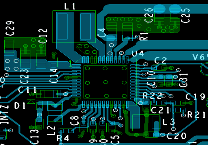
Figure 19 shows an example layout that has critical parts placed as close as possible to the pins they are connected to. Here are recommendations for the following components:
| R1 | is RLIM and is connected via a wide trace (low resistance) to the system ground. The analog ground at pin 5 should be star connected to the point where RLIM is connected to the system ground. Aim on a wide and low-ohmic trace as well, although this one is less critical (tens of mA). |
| L1 | is the big inductor for the VLED that is connected via two wide traces to the pins |
| C4 | are the decoupling capacitors for the VLED and they are as close as possible placed to the part and directly connected to ground. |
| L3/C20 | are components used for the VCORE BUCK. L3 is placed close to the pin and connected with a wide trace to the part. C20 is placed directly beside the inductor and connected to the PGND pin |
| L2 | This inductor is part of the DMD reset regulators and is also placed as close as possible to the DLPA2005 using wide PCB traces. |
10.2 Layout Example
 Figure 19. Example Layout of DLPA2005
10.3 Thermal Considerations
An important consequence of the efficiency numbers shown in Figure 7 is that it enables to perform DLPA2005 thermal calculations. Since the efficiency is not 100%, power is dissipated in the DLPA2005 chip. Due to that dissipation die temperature will rise. For reliability reasons it is good to aim for as low as possible die temperatures. Using a heat sink and airflow are efficient means to keep die temperature reasonably low. In cases that airflow and / or a heat sink are / is not feasible, the system designer should specifically pay attention to the thermal design. The die temperature for regular operation should remain below 120°C.
| In the following an example is given of such a thermal calculation. The calculation starts with summarizing all blocks in the DLPA2005 that dissipate. Clearly, the buck-boost converter supplying the LED power is the main source of dissipation. For illustrating purposes here we assume this buck-boost converter to be the only block that dissipates significantly. For the example assume: VOUT=4.8 V (for all three LEDs), IOUT=2.4 A and VIN=5 V. From Figure 7 it can be derived that the related efficiency equals about neff=88%. | ||
| The power dissipated by the DLPA2005 is then given by: |
SPACE

SPACE
The rise of die temperature due to this power dissipation can be calculated using the thermal resistance from junction to ambient, JA=27.9°C/W. This calculation yields:
SPACE

SPACE
It is also possible to calculate the maximum allowable ambient temperature to prevent surpassing the maximum die temperature. Assume again the dissipation of PDISS=1.6W. The maximum ambient temperature that is allowed is then given by:
SPACE

SPACE
It is again stressed here that for proper calculations the total power dissipation of the PAD2005 should be taken into account. On top of that, if components that are close to the PAD2005 also dissipate a significant amount of power, the (local) ambient temperature can be higher than the ambient temperature of the system.
If calculations show that the die temperature will surpass the maximum specified value, two basic options exist:
- Adding a heat sink with or without airflow. This will reduce 0JA yielding lower die temperature.
- Lowering the dissipation in the PAD2005 implying lowering the maximum allowable LED current.