| CURRENT OUTPUT |
| IOUT |
Output Current Ranges |
|
0 |
|
24 |
mA |
|
0 |
|
20 |
mA |
|
3.5 |
|
23.5 |
mA |
|
-24 |
|
24 |
mA |
|
4 |
|
20 |
mA |
| Accuracy |
|
Resolution |
|
16 |
|
|
Bits |
| INL |
Relative Accuracy(1) |
All ranges except bipolar range |
-12 |
|
12 |
LSB |
| Bipolar range only |
-16 |
|
16 |
LSB |
| DNL |
Differential Nonlinearity(1) |
Ensured monotonic |
-1 |
|
1 |
LSB |
| TUE |
Total Unadjusted Error(1) |
-40℃ to +125℃ |
-0.14 |
|
0.14 |
%FSR |
| -40℃ to +125℃, 4 to 20 mA |
-0.4 |
|
0.4 |
%FSR |
| TA = +25℃, 4 to 20 mA |
-0.2 |
|
0.2 |
%FSR |
| TA = +25°C |
-0.12 |
|
0.12 |
%FSR |
| OE |
Offset Error(1) |
-40℃ to +125℃ |
-0.1 |
|
0.1 |
%FSR |
| TA = +25°C |
-0.05 |
|
0.05 |
%FSR |
| OE-TC |
Offset Error Temperature Coefficient |
-40℃ to +125℃ |
|
4 |
|
ppm FSR/ºC |
| ZCE |
Zero Code Error |
-40℃ to +125℃, 0x0000h into DAC |
-15 |
|
15 |
uA |
| -40℃ to +125℃, 0x0000h into DAC, 4 to 20 mA |
-18 |
|
18 |
uA |
| TA = 25℃, 0x0000h into DAC |
|
1.2 |
|
m%FSR |
| TA = 25℃, 0x0000h into DAC, 4 to 20 mA |
|
1.8 |
|
m%FSR |
| ZCE-TC |
Zero Code Error Temperature Coefficient |
0x0000h into DAC, -40℃ to +125℃ |
|
4 |
|
ppm/ºC |
| GE |
Gain Error(2) |
-40℃ to +125℃ |
-0.125 |
|
0.125 |
%FSR |
| -40℃ to +125℃, 4 to 20 mA |
-0.25 |
|
0.25 |
%FSR |
| TA = +25℃, 4 to 20 mA |
-0.2 |
|
0.2 |
%FSR |
| TA = +25°C |
-0.12 |
|
0.12 |
%FSR |
| GE-TC |
Gain Error Temperature Coefficient |
-40℃ to +125℃ |
|
3 |
|
ppm FSR/ºC |
| PFSE |
Positive Full Scale Error |
0xFFFFh into DAC, -40℃ to +125℃ |
-0.125 |
|
0.125 |
%FSR |
| 0xFFFFh into DAC, -40℃ to +125℃, 4 to 20 mA |
-0.25 |
|
0.25 |
%FSR |
| 0xFFFFh into DAC, TA = 25℃ |
|
0.016 |
|
%FSR |
| 0xFFFFh into DAC, TA = 25℃, 4 to 20 mA |
|
0.024 |
|
%FSR |
| NFSE |
Negative Full Scale Error |
0x0000h into DAC, Bipolar range only, -40℃ to +125℃ |
-0.125 |
|
0.125 |
%FSR |
| 0x0000h into DAC, Bipolar range only, TA = 25℃ |
|
0.02 |
|
%FSR |
| PFSE-TC |
Positive Full Scale Error Temperature Coefficient |
|
|
5 |
|
ppm FSR/ºC |
| NFSE-TC |
Negative Full Scale Error Temperature Coefficient |
Bipolar range only |
|
5 |
|
ppm FSR/ºC |
| BPZE |
Bipolar Zero Error |
Bipolar range only, 0x8000h into DAC -40℃ to +125℃ |
-0.05 |
|
0.05 |
%FSR |
| Bipolar range only, 0x8000h into DAC, TA = +25°C |
-0.02 |
|
0.02 |
| BPZE-TC |
Bipolar Zero Error Temperature Coefficient |
0x8000h into DAC,-40℃ to +125℃ |
|
4 |
|
ppm/ºC |
| VCL |
Compliance Voltage |
Output = 24 mA |
|
|
VPOS_IN_x-3 |
V |
| Output = ±24 mA |
|VNEG_IN_x|+3 |
|
VPOS_IN_x-3 |
V |
| RL |
Resistive Load |
All except ±24 mA range |
|
|
1.2 |
KΩ |
| ±24 mA range |
|
|
0.625 |
| DC-PSRR |
DC Power Supply Rejection Ratio |
Code = 0x8000, 20 mA range |
|
0.1 |
|
µA/V |
| ZO |
Output Impedance |
Code = 0x8000 |
|
10 |
|
MΩ |
| IOLEAK |
Output Current Leakage |
Iout is disabled or in power-down |
|
1 |
|
nA |
| HART INTERFACE |
| VHART-IN |
HART Input |
|
400 |
500 |
600 |
mVpp |
|
Corresponding Output |
HART In = 500 mVpp 1.2 KHz |
|
1 |
|
mApp |
| VOLTAGE OUTPUT |
| VOUT |
Voltage Output Ranges (normal mode) |
|
0 |
|
5 |
V |
| 0 |
|
10 |
V |
| -5 |
|
5 |
V |
| -10 |
|
10 |
V |
| Voltage Output Ranges (Overrange mode) |
|
0 |
|
6 |
V |
| 0 |
|
12 |
V |
| -6 |
|
6 |
V |
| -12 |
|
12 |
V |
| Accuracy |
|
Resolution |
|
16 |
|
|
Bits |
| INL |
Relative Accuracy, INL(1) |
|
-12 |
|
12 |
LSB |
| DNL |
Differential Nonlinearity, DNL(1) |
Ensured monotonic |
-1 |
|
1 |
LSB |
| TUE |
Total Unadjusted Error, TUE(1) |
-40℃ to +125℃, VOUT unloaded |
-0.1 |
±0.05 |
0.1 |
%FSR |
| TA = +25°C, VOUT unloaded |
-0.075 |
|
0.075 |
%FSR |
| ZCE |
Zero Code Error(5) |
Unipolar ranges only, VOUT unloaded, -40℃ to +125℃ |
-2.5 |
|
2.5 |
mV |
| Unipolar ranges only, VOUT unloaded, TA = 25℃ |
|
0.14 |
|
mV |
| ZCE-TC |
Zero Code Error Temperature Coefficient |
Unipolar ranges only, -40℃ to +125℃ |
|
2 |
|
ppm FSR/ºC |
| BPZE |
Bipolar Zero Error |
Bipolar range only, 0x8000h into DAC -40℃ to +125℃, VOUT unloaded |
-0.03 |
|
0.03 |
%FSR |
| Bipolar range only, 0x8000h into DAC, TA = +25°C, VOUT unloaded |
-0.025 |
|
0.025 |
%FSR |
| BPZE-TC |
Bipolar Zero Error Temperature Coefficient |
Bipolar range only, 0x8000h into DAC, -40℃ to +125℃, VOUT unloaded |
|
1 |
|
ppm FSR/ºC |
| GE |
Gain Error(1) |
-40℃ to +125℃, VOUT unloaded |
-0.1 |
|
0.1 |
%FSR |
| TA = +25°C, VOUT unloaded |
-0.07 |
|
0.07 |
%FSR |
| GE-TC |
Gain Error Temperature Coefficient |
-40℃ to +125℃ |
|
3 |
|
ppm FSR/ºC |
| PFSE |
Positive Full Scale Error |
0xFFFFh into DAC, -40℃ to +125℃, VOUT unloaded |
-0.1 |
|
0.1 |
%FSR |
| 0xFFFFh into DAC, TA = 25℃, VOUT unloaded |
|
0.03 |
|
%FSR |
| NFSE |
Negative Full Scale Error(5) |
Bipolar ranges only, 0x0000h into DAC, -40℃ to +125℃, VOUT unloaded |
-0.06 |
|
0.06 |
%FSR |
| Bipolar ranges only, 0x0000h into DAC, TA = 25℃, VOUT unloaded |
|
0.002 |
|
%FSR |
| PFSE-TC |
Positive Full Scale Error Temperature Coefficient |
VOUT unloaded, -40℃ to +125℃ |
|
2 |
|
ppm FSR/ºC |
| NFSE-TC |
Negative Full Scale Error Temperature Coefficient |
VOUT unloaded, -40℃ to +125℃ |
|
2 |
|
ppm FSR/ºC |
|
Headroom |
Output unloaded, VPOS_IN_x with respect to VOUT_x, 0xFFFFh into DAC, No load |
0.5 |
|
|
V |
| Output unloaded, VPOS_IN_x with respect to VOUT_x, 0xFFFFh into DAC, 1 kΩ load |
3 |
|
|
V |
|
Footroom |
Bipolar, ranges only, VNEG_IN_x with respect to VOUT_x, 0x0000h into DAC |
3 |
|
|
V |
| Unipolar ranges only, VNEG_IN_x with respect to VOUT_x, 0x0000h into DAC |
5 |
|
|
V |
|
Short-Circuit Current |
SCLIM[1:0] = "00" (see register map) |
17 |
|
23 |
mA |
| SCLIM[1:0] = "01" (see register map) |
8 |
|
11 |
mA |
| SCLIM[1:0] = "10" (see register map) |
22 |
|
28 |
mA |
| SCLIM[1:0] = "11" (see register map) |
26 |
|
34 |
mA |
| RL |
Load |
|
1 |
|
|
kΩ |
| CL |
Capacitive Load Stability |
RL = Open |
|
|
20 |
nF |
| RL = 1 kΩ |
|
|
20 |
nF |
| RL = 1 kΩ with External compensation capacitor (150 pF) connected |
|
|
1 |
µF |
| ZO |
DC Output Impedance |
Voltage output enabled, VOUT = Mid Scale, UP10V range |
|
0.01 |
|
Ω |
| Voltage output disabled (POC = '1') |
|
50 |
|
MΩ |
| Voltage output disabled (POC = '0') |
|
30 |
|
kΩ |
| ILEAK |
Output Leakage (VOUT_x Pin) |
Voltage output disabled (POC = '1') |
|
1 |
|
nA |
| DC-PSRR |
DC Power Supply Rejection Ratio |
No output load |
|
10 |
|
µV/V |
|
VSENSEP Impedance |
VOUT enabled Mid-Scale UP10 |
|
240 |
|
kΩ |
|
VSENSEN Impedance |
VOUT enabled Mid-Scale UP10 |
|
120 |
|
kΩ |
| EXTERNAL REFERENCE INPUT |
| IREF |
External Reference Current |
VOUT = Full scale, BP12V range, per channel |
|
0.35 |
|
mA |
|
Reference Input Capacitance |
|
|
100 |
|
pF |
| INTERNAL REFERENCE OUTPUT |
| VREF |
Reference Output |
TA = 25°C |
4.99 |
|
5.01 |
V |
| VREF-TC |
Reference TC |
TA = -40℃ to +125℃ |
-13 |
|
13 |
ppm/°C |
| TA = -25℃ to +125℃ |
-10 |
|
10 |
ppm/°C |
| TUE |
DAC Voltage Output Total Unadjusted Error(1) |
-40°C to +125°C, VOUT_x unloaded, Internal reference enabled |
|
0.2 |
|
%FSR |
| DAC Current Output Total Unadjusted Error(1) |
-40°C to +125°C, Internal reference enabled |
|
0.2 |
|
%FSR |
| -40°C to +125°C, Internal reference enabled, 4 mA to 20 mA range |
|
0.5 |
|
%FSR |
|
Output Noise (0.1 Hz to 10 Hz) |
TA = 25°C |
|
13 |
|
µV p-p |
|
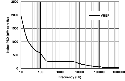
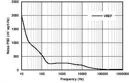
Noise Spectral Density |
At 10 kHz, At 25°C |
|
200 |
|
nV/sqrtHz |
| CL |
Capacitive Load |
|
|
|
600 |
nF |
| IL |
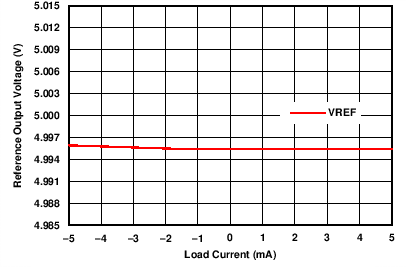
Load Current |
|
|
±5 |
|
mA |
|
Short Circuit Current |
Ref-Out shorted to PBKG |
|
20 |
|
mA |
|
Load Regulation |
Sourcing and Sinking, TA = +25°C |
|
5 |
|
µV/mA |
|
Line Regulation |
TA = +25°C |
|
2 |
|
uV/V |
| BUCK BOOST CONVERTER |
| RON |
Switch On Resistanvce |
TA = +25°C |
|
3 |
|
Ω |
| ILEAK |
Switch Leakage Current |
TA = +25°C |
|
20 |
|
nA |
| L |
Inductor |
Between LP_x and LN_x |
|
100 |
|
µH |
| ILMAX |
Peak Inductor Current |
TA = +25°C, PVDD = AVDD = 36 V, Buck-Boost Converter enabled |
|
|
0.5 |
A |
| VO |
Output Voltage |
VPOS_IN_x minimum |
|
4 |
|
V |
| VPOS_IN_x maximum |
|
32 |
|
V |
| VO |
Output Voltage |
VNEG_IN_x minimum |
|
-18 |
|
V |
| VNEG_IN_x maximum |
|
-5 |
|
V |
| CL |
Load Capacitor |
VPOS_IN_x and VNEG_IN_x |
10 |
|
|
µF |
|
Start Up Time |
After enabling VPOS_IN_x and VNEG_IN_x with 10 µF load capacitor on these pins |
|
3 |
|
ms |
| DVDD LDO |
| VO |
Output Voltage |
|
|
5 |
|
V |
| ILOAD |
Load Current |
|
|
|
10 |
mA |
| CL |
Load Capacitor |
|
|
|
0.2 |
nF |
| THERMAL ALARM |
|
Trip Point |
|
|
150 |
|
°C |
|
Hysteresis |
|
|
15 |
|
°C |
| DIGITAL INPUTS |
|
Hysteresis Voltage |
|
|
0.4 |
|
V |
|
Input Current |
|
-5 |
|
5 |
µA |
|
Input Current (DVDD_EN) |
|
-10 |
|
10 |
µA |
|
Pin Capacitance |
Per pin |
|
10 |
|
pF |
| DIGITAL OUTPUTS |
| SDO |
| VOL |
Output Low Voltage |
Sinking 200 µA |
|
|
0.4 |
V |
| VOH |
Output High Voltage |
Sourcing 200 µA |
DVDD-0.5 |
|
|
V |
| ILEAK |
High Impedance Leakage |
|
-5 |
|
5 |
µA |
|
High Impedance Output Capacitance |
|
|
10 |
|
pF |
| ALARM |
| VOL |
Output Low Voltage |
At 2.5 mA |
|
0.4 |
|
V |
| ILEAK |
High Impedance Leakage |
|
|
50 |
|
µA |
|
High Impedance Output Capacitance |
|
|
10 |
|
pF |
| POWER REQUIREMENTS |
| IAVDD+IPVDD |
Current Flowing into AVDD and PVDD |
All Buck-Boost converter positive output enabled, IOUT_x mode operation, All IOUT channels enabled, 0 mA, PVDD = AVDD = 12 V, Internal reference, VNEG_IN_x = 0 V |
|
5 |
|
mA |
| All IOUT Active, 0 mA, 0 to 24 mA range, VNEG_IN_x = 0 V |
|
3.5 |
5 |
mA |
| IPVDD_x |
Current Flowing into PVDD |
Buck-Boost converter enabled, Peak current |
|
|
0.5 |
A |
| Buck-Boost converter disabled |
|
0.1 |
|
mA |
| IDVDD |
Current Flowing into DVDD |
All digital pins at DVDD, DVDD = 5.5 V |
|
1.8 |
|
mA |
| IVPOS_IN_x |
Current Flowing into VPOS_IN_x |
IOUT active, 0 mA, 0 to 24 mA range |
|
|
1.2 |
mA |
| VOUT active, No load, 0 to 10 V range, Mid scale code |
|
|
3 |
mA |
| IVNEG_IN_x |
Current Flowing into VNEG_IN_x |
IOUT active, 0 mA, ±24 mA range |
|
|
1.2 |
mA |
| VOUT active, No load, 0 to 10 V range, Mid scale code |
|
|
3 |
mA |
| PDISS |
Power Dissipation (PVDD+AVDD) |
All Buck-Boost converter positive output enabled, IOUT_x mode operation, All IOUT channels enabled, Rload = 1 Ω, 24 mA, PVDD = AVDD = 12 V, Internal reference, VNEG_IN_x = 0 V |
|
0.86 |
1.1 |
W |
| IVSENSEP |
Current Flowing into VSENSEP |
VOUT disabled |
|
|
40 |
nA |
| IVSENSEN |
Current Flowing into VSENSEN |
VOUT disabled |
|
|
20 |
nA |
| DYNAMIC PERFORMANCE |
| Voltage Output |
| Tsett |
Output Voltage Settling Time |
0 to10 V, to ±0.03% FSR RL = 1K||CL = 200 pF |
|
15 |
|
µs |
| 0 to 5 V, to ±0.03% FSR RL = 1K||CL = 200 pF |
|
10 |
|
µs |
| -5 to 5 V, to ±0.03% FSR RL = 1K||CL = 200 pF |
|
15 |
|
µs |
| -10 to 10 V, to ±0.03% FSR RL = 1K||CL = 200 pF |
|
30 |
|
µs |
|
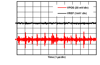
Output Voltage Ripple |
Buck-Boost converter enabled, 50 KHz, 20dB/decade filter on VPOS_IN_x |
|
2 |
|
mVpp |
| SR |
Slew Rate |
RL = 1K||CL = 200 pF |
|
1 |
|
V/µs |
|
Power-On Glitch Magnitude(2) |
|
|
0.1 |
|
V |
|
Power-off Glitch Magnitude(3) |
|
|
0.8 |
|
V |
|
Channel to Channel DC Crosstalk |
Full scale swing on adjacent channel |
|
2 |
|
m%FSR |
|
Code-to-Code Glitch |
|
|
0.15 |
|
µV-sec |
|
Digital Feedthrough |
|
|
1 |
|
nV-sec |
|
Output Noise (0.1 Hz to 10 Hz bandwidth) |
UP10V, Mid scale |
|
0.1 |
|
LSB p-p |
|
Output Noise (100 kHz bandwidth) |
UP10V, Mid scale |
|
200 |
|
µVrms |
|
Output Noise Spectral Density |
BP20V Measured at 10 kHz, Mid scale |
|
200 |
|
nV/sqrtHz |
| AC-PSRR |
AC Power Supply Rejection Ratio |
200 mV 50/60Hz Sine wave superimposed on power supply voltage. (AC analysis) |
|
-75 |
|
dB |
| Current Output |
| Tsett |
Output Current Settling Time |
24 mA Step, to 0.1% FSR, no L |
|
10 |
|
µs |
| 24 mA Step, to 0.1% FSR , L = 1 mH, CL = 22 nF |
|
50 |
|
µs |
|
Output Current Ripple |
Buck-Boost converter enabled, 50 KHz, 20dB/decade filter on VPOS_IN_x |
|
8 |
|
µApp |
| L |
Inductive Load(4) |
|
|
|
50 |
mH |
| AC-PSRR |
AC Power Supply Rejection Ratio |
200 mV 50/60Hz Sine wave superimposed on power supply voltage. |
|
-75 |
|
dB |
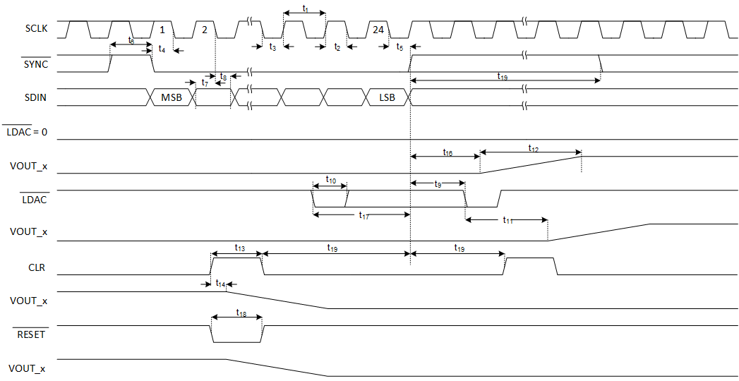 Figure 1. Write Mode Timing
 Figure 2. Readback Mode Timing
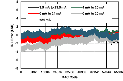
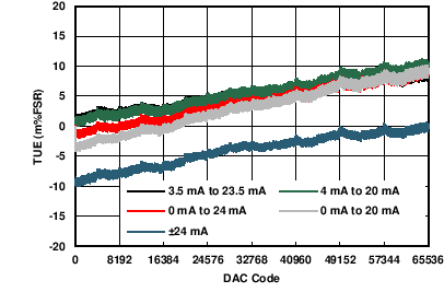
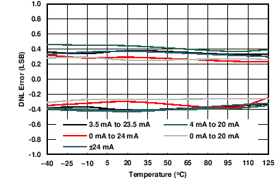
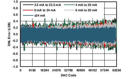
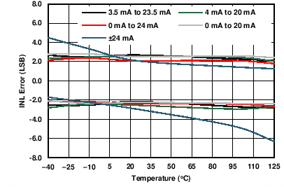
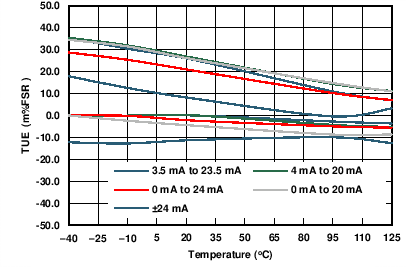

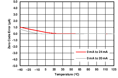
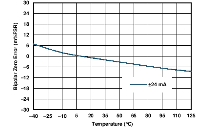
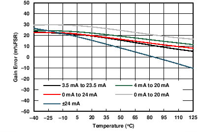
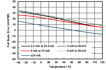
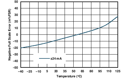
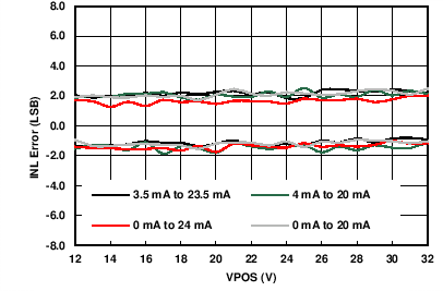
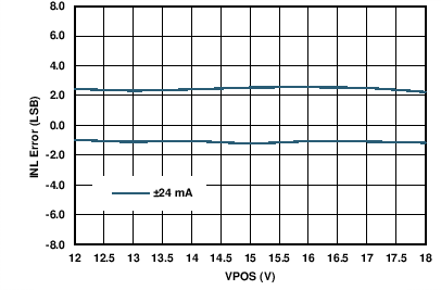
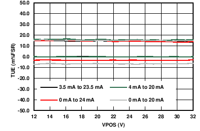
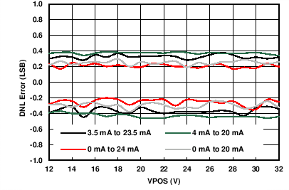
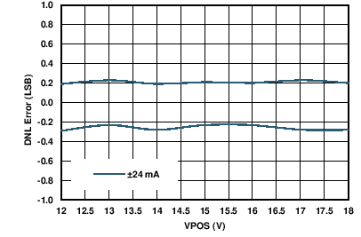
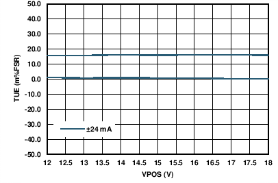
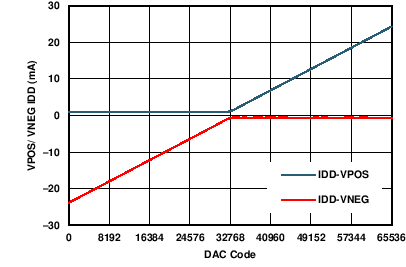
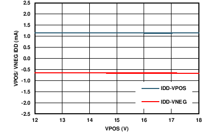

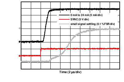

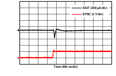
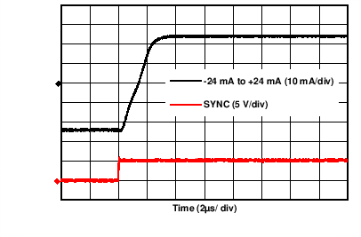
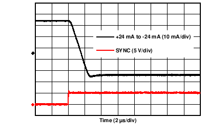
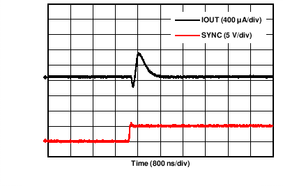
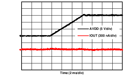
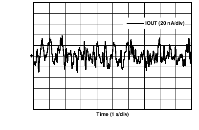
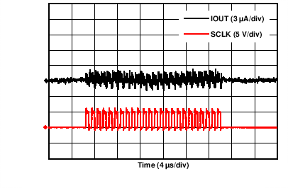
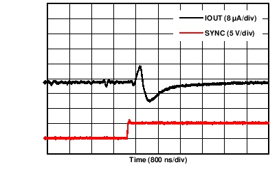
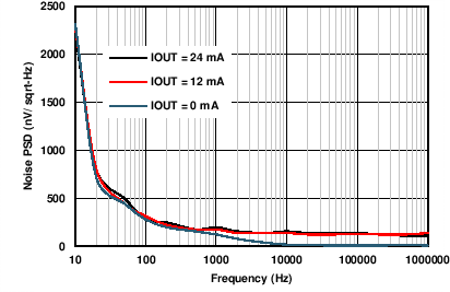
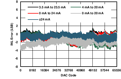
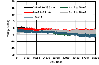
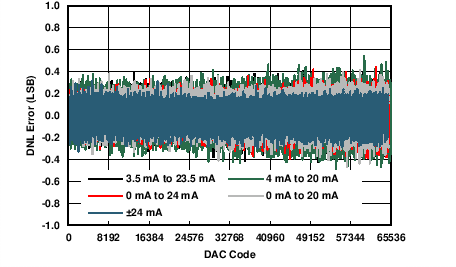
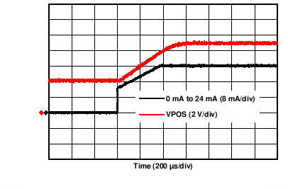
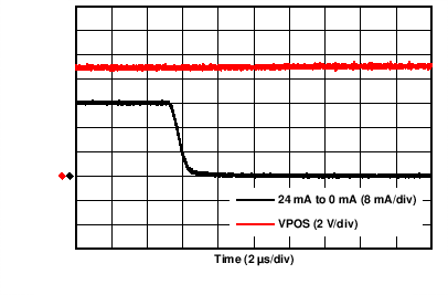
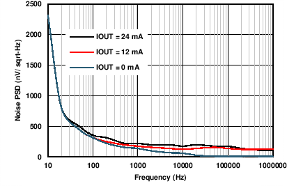
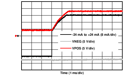
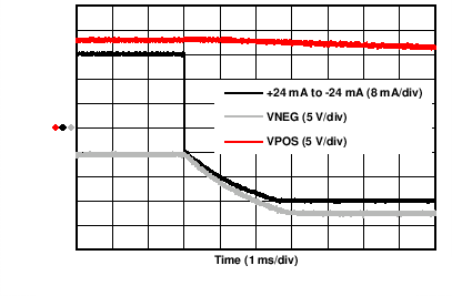
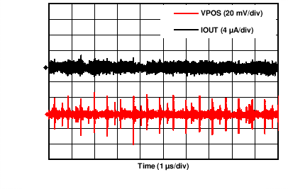
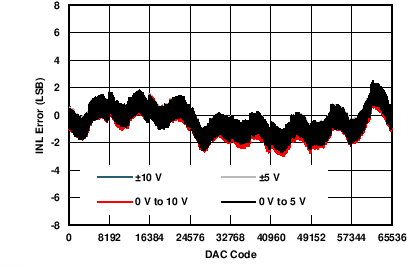
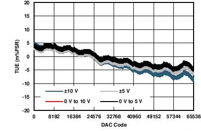
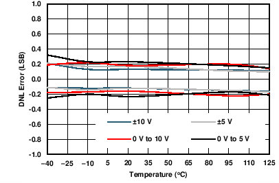
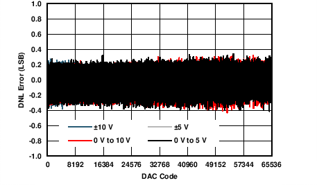
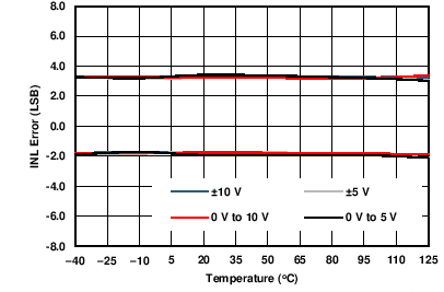
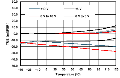
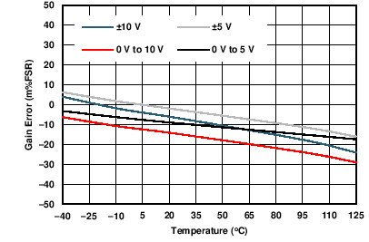
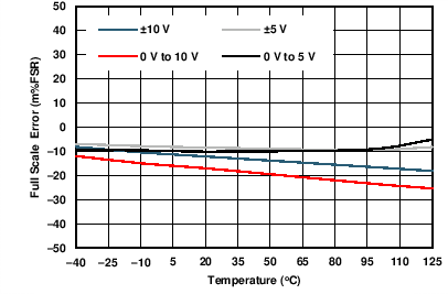

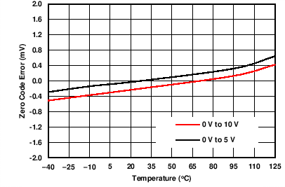
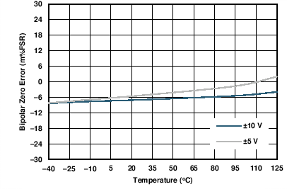
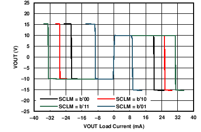
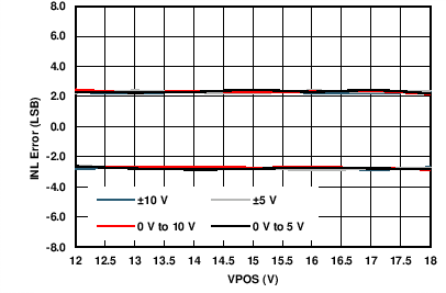
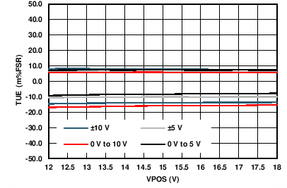
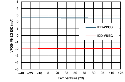
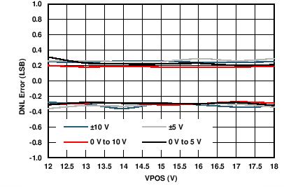
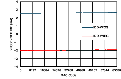
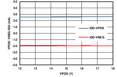
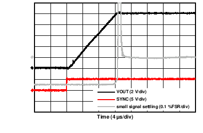
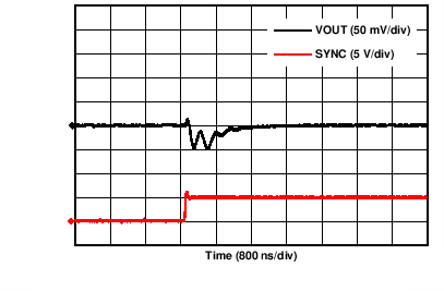
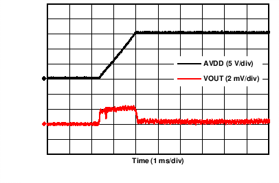
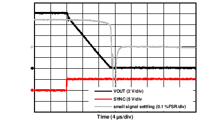
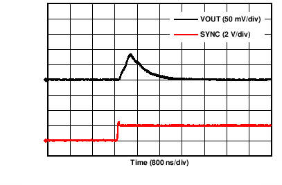
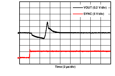
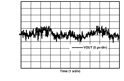
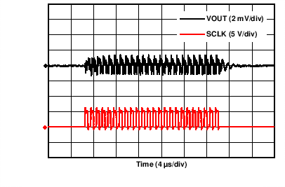
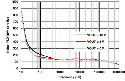
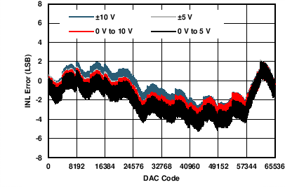
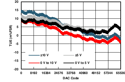
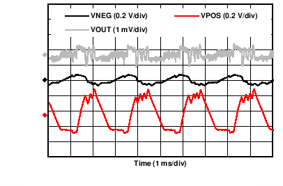
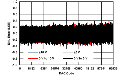
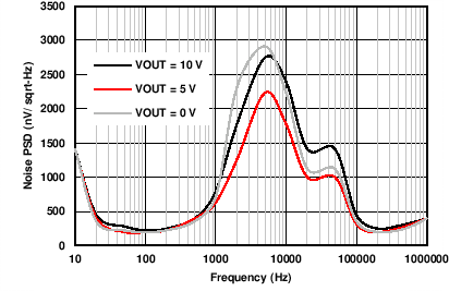
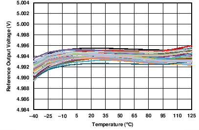
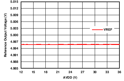
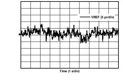 Figure 80. Internal Reference Noise, 0.1 Hz to 10 Hz
