SBAS246B December 2001 – November 2014 DAC8532
PRODUCTION DATA.
- 1 Features
- 2 Applications
- 3 Description
- 4 Simplified Diagram
- 5 Revision History
- 6 Pin Configuration and Functions
- 7 Specifications
- 8 Detailed Description
-
9 Application and Implementation
- 9.1 Application Information
- 9.2 Typical Application
- 10Power Supply Recommendations
- 11Layout
- 12Device and Documentation Support
- 13Mechanical, Packaging, and Orderable Information
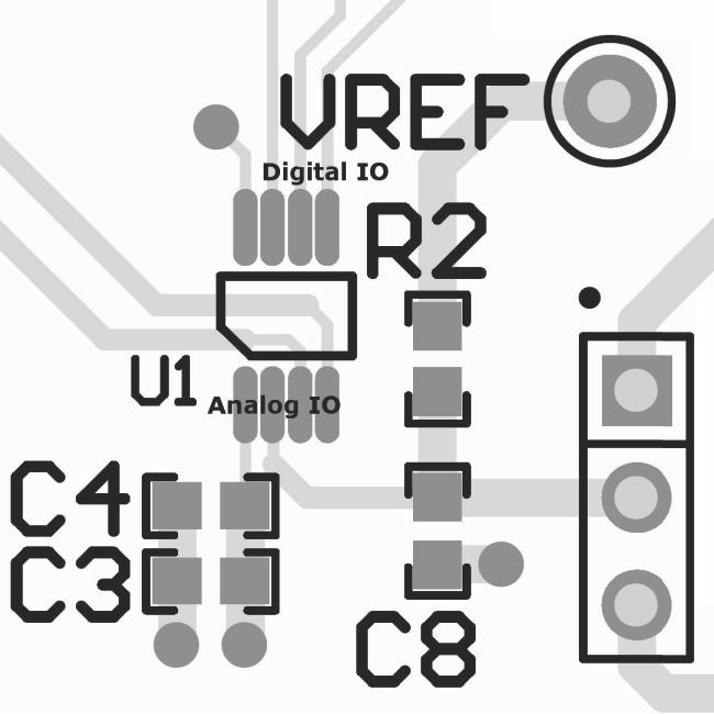
11 Layout
11.1 Layout Guidelines
A precision analog component requires careful layout, adequate bypassing, and clean, well-regulated power supplies.
The DAC8532 offers single-supply operation, and it will often be used in close proximity with digital logic, microcontrollers, microprocessors, and digital signal processors. The more digital logic present in the design and the higher the switching speed, the more difficult it will be to keep digital noise from appearing at the output.
Due to the single ground pin of the DAC8532, all return currents, including digital and analog return currents for the DAC, must flow through a single point. Ideally, GND would be connected directly to an analog ground plane. This plane would be separate from the ground connection for the digital components until they were connected at the power entry point of the system.
The power applied to VDD should be well regulated and low noise. Switching power supplies and DC/DC converters will often have high-frequency glitches or spikes riding on the output voltage. In addition, digital components can create similar high-frequency spikes as their internal logic switches states. This noise can easily couple into the DAC output voltage through various paths between the power connections and analog output.
As with the GND connection, VDD should be connected to a positive power-supply plane or trace that is separate from the connection for digital logic until they are connected at the power entry point. In addition, a 1 µF to 10 µF capacitor in parallel with a 0.1 µF bypass capacitor is strongly recommended. In some situations, additional bypassing may be required, such as a 100 µF electrolytic capacitor or even a Pi filter made up of inductors and capacitors—all designed to low-pass filter the supply, removing the high-frequency noise.
11.2 Layout Example