ZHCSHR4F January 2009 – April 2018 DAC7568 , DAC8168 , DAC8568
PRODUCTION DATA.
- 1 特性
- 2 应用
- 3 说明
- 4 修订历史记录
- 5 Device Comparison Table
- 6 Pin Configuration and Functions
- 7 Specifications
-
8 Detailed Description
- 8.1 Functional Block Diagram
- 8.2
Feature Description
- 8.2.1 Digital-to-Analog Converter (DAC)
- 8.2.2 Resistor String
- 8.2.3 Output Amplifier
- 8.2.4 Internal Reference
- 8.2.5 Serial Interface
- 8.2.6 Input Shift Register
- 8.2.7 SYNC Interrupt
- 8.2.8 Power-on Reset to Zero Scale or Midscale
- 8.2.9 Clear Code Register and CLR Pin
- 8.2.10 Software Reset Function
- 8.2.11
Operating Examples: DAC7568/DAC8168/DAC8568
- Table 4. 1st: Write to Data Buffer A:
- Table 5. 2nd: Write to Data Buffer B:
- Table 6. 3rd: Write to Data Buffer G:
- Table 7. 4th: Write to Data Buffer H and Simultaneously Update all DACs:
- Table 8. 1st: Write to Data Buffer C and Load DAC C: DAC C Output Settles to Specified Value Upon Completion:
- Table 9. 2nd: Write to Data Buffer D and Load DAC D: DAC D Output Settles to Specified Value Upon Completion:
- Table 10. 3rd: Write to Data Buffer E and Load DAC E: DAC E Output Settles to Specified Value Upon Completion:
- Table 11. 4th: Write to Data Buffer F and Load DAC F: DAC F Output Settles to Specified Value Upon Completion:
- Table 12. 1st: Write Power-Down Command to DAC Channel A and DAC Channel B: DAC A and DAC B to 1kΩ.
- Table 13. 2nd: Write Power-Down Command to DAC Channel H: DAC H to 1kΩ.
- Table 14. 3rd: Write Power-Down Command to DAC Channel C and DAC Channel D: DAC C and DAC D to 100kΩ.
- Table 15. 4th: Write Power-Down Command to DAC Channel F: DAC F to 100kΩ.
- Table 16. 1st: Write Sequence for Enabling the DAC7568, DAC8168, and DAC8568 Internal Reference All the Time:
- Table 17. 2nd: Write Sequence to Power-Down All DACs to High-Impedance:
- Table 18. 1st: Write Sequence for Disabling the DAC7568, DAC8168, and DAC8568 Internal Reference All the Time (after this sequence, these devices require an external reference source to function):
- Table 19. 2nd: Write Sequence to Write Specified Data to All DACs:
- 8.3
Device Functional Modes
- 8.3.1
Enable/Disable Internal Reference
- 8.3.1.1 Static Mode
- 8.3.1.2
Flexible Mode
- Table 22. Write Sequence for Enabling Internal Reference (Flexible Mode) (Internal Reference Powered On—09080000h)
- Table 23. Write Sequence for Enabling Internal Reference (Flexible Mode) (Internal Reference Always Powered On—090A0000h)
- Table 24. Write Sequence for Disabling Internal Reference (Flexible Mode) (Internal Reference Always Powered Down—090C0000h)
- Table 25. Write Sequence for Switching from Flexible Mode to Static Mode for Internal Reference (Internal Reference Always Powered Down—09000000h)
- 8.3.2 LDAC Functionality
- 8.3.3 Power-Down Modes
- 8.3.1
Enable/Disable Internal Reference
-
9 Application and Implementation
- 9.1 Application Information
- 9.2
Typical Applications - Microprocessor Interfacing
- 9.2.1 DAC7568/DAC8168/DAC8568 to an 8051 Interface
- 9.2.2 DAC7568/DAC8168/DAC8568 to Microwire Interface
- 9.2.3 DAC7568/DAC8168/DAC8568 to 68HC11 Interface
- 10Layout
- 11器件和文档支持
- 12机械、封装和可订购信息
9.2.1.1.1 Internal Reference
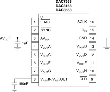
The internal reference of the DAC7568, DAC8168, and DAC8568 does not require an external load capacitor for stability because it is stable with any capacitive load. However, for improved noise performance, an external load capacitor of 150nF or larger connected to the VREFH/VREFOUT output is recommended. Figure 126 shows the typical connections required for operation of the DAC7568, DAC8168, and DAC8568 internal reference. A supply bypass capacitor at the AVDD input is also recommended.
 Figure 126. Typical Connections for Operating the DAC7568/DAC8168/DAC8568 Internal Reference (16-Pin Version Shown)