ZHCSH64D June 2017 – August 2018 DAC60508 , DAC70508 , DAC80508
PRODUCTION DATA.
- 1 特性
- 2 应用
- 3 说明
- 4 修订历史记录
- 5 Device Comparison Table
- 6 Pin Configuration and Functions
- 7 Specifications
-
8 Detailed Description
- 8.1 Overview
- 8.2 Functional Block Diagram
- 8.3 Feature Description
- 8.4 Device Functional Modes
- 8.5 Programming
- 8.6
Register Map
- 8.6.1 NOP Register (address = 0x00) [reset = 0x0000]
- 8.6.2 DEVICE ID Register (address = 0x01) [reset = 0x---]
- 8.6.3 SYNC Register (address = 0x2) [reset = 0xFF00]
- 8.6.4 CONFIG Register (address = 0x3) [reset = 0x0000]
- 8.6.5 GAIN Register (address = 0x04) [reset = 0x---]
- 8.6.6 TRIGGER Register (address = 0x05) [reset = 0x0000]
- 8.6.7 BRDCAST Register (address = 0x6) [reset = 0x0000]
- 8.6.8 STATUS Register (address = 0x7) [reset = 0x0000]
- 8.6.9 DACx Register (address = 0x8 to 0xF) [reset = 0x0000 or 0x8000]
- 9 Application and Implementation
- 10Power Supply Recommendations
- 11Layout
- 12器件和文档支持
- 13机械、封装和可订购信息
封装选项
机械数据 (封装 | 引脚)
散热焊盘机械数据 (封装 | 引脚)
- RTE|16
订购信息
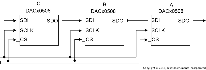
8.4.2 Daisy-Chain Operation
For systems that contain more than one DACx0508 devices, the SDO pin can be used to daisy-chain them together. Daisy-chain operation is useful in reducing the number of serial interface lines.
The first falling edge on the CS pin starts the operation cycle. If more than 24 SCLK pulses are applied while the CS pin is kept low, the data ripples out of the shift register and is clocked out on the SDO pin either on the falling edge or rising edge of SCLK according to the FSDO bit. By connecting the SDO output of the first device to the SDI input of the next device in the chain, a multiple-device interface is constructed. Each device in the system requires 24 clock pulses. As a result the total number of clock cycles must be equal to 24 × N, where N is the total number of DACx0508 devices in the daisy chain. When the serial transfer to all devices is complete the CS signal is taken high. This action transfers the data from the serial peripheral interface (SPI) shift registers to the internal registers of each device in the daisy chain and prevents any further data from being clocked into the input shift register.
 Figure 64. Daisy-Chain Layout