ZHCSF34D April 2016 – December 2017 DAC60004 , DAC70004 , DAC80004
PRODUCTION DATA.
- 1 特性
- 2 应用
- 3 说明
- 4 修订历史记录
- 5 Device Comparison Table
- 6 Pin Configuration and Functions
- 7 Specifications
-
8 Detailed Description
- 8.1 Overview
- 8.2 Functional Block Diagram
- 8.3 Feature Description
- 8.4 Device Functional Modes
- 9 Application and Implementation
- 10Power Supply Recommendations
- 11Layout
- 12器件和文档支持
- 13机械、封装和可订购信息
封装选项
机械数据 (封装 | 引脚)
散热焊盘机械数据 (封装 | 引脚)
- DMD|14
订购信息
7 Specifications
7.1 Absolute Maximum Ratings
over operating free-air temperature range (unless otherwise noted) (1)| MIN | MAX | UNIT | ||
|---|---|---|---|---|
| Voltage, VDD to GND | –0.3 | 7 | V | |
| Voltage, digital input or output to GND | –0.3 | VDD + 0.3 | V | |
| Voltage, analog input (REFIN) or output (VOUTx) to GND | –0.3 | VDD + 0.3 | V | |
| Input current to any pin except supply pins | –10 | 10 | mA | |
| Maximum junction temperature | 150 | °C | ||
| Storage temperature range, Tstg | -60 | 150 | °C | |
(1) Stresses beyond those listed under Absolute Maximum Ratings may cause permanent damage to the device. These are stress ratings only, which do not imply functional operation of the device at these or any other conditions beyond those indicated under Recommended Operating Conditions. Exposure to absolute-maximum-rated conditions for extended periods may affect device reliability.
7.2 ESD Ratings
| VALUE | UNIT | |||
|---|---|---|---|---|
| V(ESD) | Electrostatic discharge | Human body model (HBM), per ANSI/ESDA/JEDEC JS-001, all pins(1) | ±2000 | V |
| Charged device model (CDM), per JEDEC specification JESD22-C101, all pins(2) | ±1000 | |||
(1) JEDEC document JEP155 states that 500-V HBM allows safe manufacturing with a standard ESD control process.
(2) JEDEC document JEP157 states that 250-V CDM allows safe manufacturing with a standard ESD control process.
7.3 Recommended Operating Conditions
over operating free-air temperature range (unless otherwise noted)| MIN | NOM | MAX | UNIT | ||
|---|---|---|---|---|---|
| Voltage, VDD to GND | 2.7 | 5.5 | V | ||
| Voltage, analog input (REFIN) or output (VOUTx) to GND | 2.7 V ≤ VDD ≤ 4.5 V | 2.2 | VDD – 0.2 | V | |
| 4.5 V ≤ VDD ≤ 5.5 V | 2.2 | VDD | V | ||
| Ambient Operating Temperature, TA | -40 | 125 | °C | ||
7.4 Thermal Information
| THERMAL METRIC(1) | DACx0004 | UNIT | ||
|---|---|---|---|---|
| DMD (VSON) | PW (TSSOP) | |||
| 14 PINS | 14 PINS | |||
| RθJA | Junction-to-ambient thermal resistance | 39.6 | 99.1 | °C/W |
| RθJC(top) | Junction-to-case (top) thermal resistance | 27.3 | 23.4 | °C/W |
| RθJB | Junction-to-board thermal resistance | 9.0 | 42.8 | °C/W |
| ψJT | Junction-to-top characterization parameter | 0.3 | 0.9 | °C/W |
| ψJB | Junction-to-board characterization parameter | 8.9 | 42.0 | °C/W |
| RθJC(bot) | Junction-to-case (bottom) thermal resistance | 6.5 | N/A | °C/W |
(1) For more information about traditional and new thermal metrics, see the Semiconductor and IC Package Thermal Metrics application report.
7.5 Electrical Characteristics
All minimum/maximum specifications at TA = -40°C to +125°C, 2.7 V ≤ VDD ≤ 5.5 V, 2.5 V ≤ REFIN(4) ≤ VDD, Rload = 5 kΩ to GND, Cload = 200 pF to GND (unless otherwise noted), Digital inputs held at 0 V| PARAMETER | TEST CONDITIONS | MIN | TYP | MAX | UNIT | |
|---|---|---|---|---|---|---|
| STATIC PERFORMANCE(2) | ||||||
| Resolution | DAC80004 | 16 | Bits | |||
| DAC70004 | 14 | |||||
| DAC60004 | 12 | |||||
| INL | Relative accuracy(1) | ±1 | LSB | |||
| DNL | Differential nonlinearity(1) | Ensured monotonic | ±1 | LSB | ||
| TUE | Total unadjusted error(1) | TA = +20°C to +40°C | 1.5 | mV | ||
| TA = –40°C to +125°C | 2 | |||||
| ZCE | Zero code error | TA = –40°C to +125°C, Code 0d into DAC | ±0.2 | ±2 | mV | |
| TA = +25°C, Code 0d into DAC | ±0.1 | |||||
| ZCE-TC | Zero code error TC | TA = –40°C to +125°C | ±5 | µV/°C | ||
| OE | Offset error(1) | TA = +20°C to +40°C | ±1.2 | mV | ||
| TA = –40°C to +125°C | ±0.2 | ±1.8 | ||||
| TA = +25°C | ±0.2 | |||||
| OE-TC | Offset error drift | TA = –40°C to +125°C | ±4 | µV/°C | ||
| FSE | Full-scale error(5) | TA = +20°C to +40°C, Code 65535d into DAC | ±0.05 | %FSR | ||
| TA = –40°C to +125°C, Code 65535d into DAC | ±0.01 | ±0.07 | %FSR | |||
| TA = +25°C | ±0.01 | |||||
| FSE-TC | Full-scale error drift(5) | TA = –40°C to +125°C | ±2 | ppm FSR/°C | ||
| GE | Gain error(1) | TA = –40°C to +125°C | ±0.005 | ±0.05 | %FSR | |
| TA = +25°C | ±0.005 | |||||
| GE-TC | Gain drift | TA = –40°C to +125°C | ±2 | ppm FSR/°C | ||
| Output voltage drift vs.Time | TA = +25°C, Vout = ¾ of full scale, 1900 hr | 20 | ppm FSR | |||
| Load Regulation | TA = +25°C, Vout =Mid Scale | 0.003% | ||||
| PSRR | DC Power supply rejection ratio(5) | TA = +25°C, Vout = full scale | –92 | dB | ||
| DYNAMIC PERFORMANCE | ||||||
| Output voltage settling time | ¼ to ¾ scale and ¾ to ¼ scale settling to ±1 LSB, RL = 5 kΩ, Cload = 200 pF to GND | 5.8 | 8 | µs | ||
| Slew rate | 1.5 | V/µs | ||||
| Power-up time(3) | 100 | µs | ||||
| Power-on glitch energy | Supply slew rate <5 V/msec | 8 | mV | |||
| Power-off glitch energy | DAC in power down mode (1 kΩ-GND), Supply slew rate <5 V/msec | 7 | mV | |||
| Output noise | 0.1 Hz to 10 Hz | 5 | µVpp | |||
| 100 kHz BW | 100 | µVRMS | ||||
| Output noise density | Measured at 1 kHz | 60 | nV/√Hz | |||
| Measured at 10 kHz | 55 | |||||
| THD | Total harmonic distortion | REFIN = 3 V ± 0.2 Vpp, Frequency = 10 kHz, DAC at mid scale, specified by design | –80 | dB | ||
| PSRR | AC power supply rejection ratio | 200 mV 50 Hz and 60 Hz sine wave superimposed on power supply voltage (AC analysis) | -90 | dB | ||
| Code change glitch impulse | 1 LSB change around major carry, Software LDAC mode | 1 | nV-s | |||
| Channel-to-channel AC (analog) crosstalk | Full-scale swing on adjacent channel, Hardware LDAC mode | 1 | nV-s | |||
| Channel-to-channel DC crosstalk | Full-scale swing on adjacent channels, Measured channel at zero scale | 1 | LSB | |||
| Full-scale swing on all channel, Measured channel at zero scale | 1 | |||||
| Digital crosstalk | DAC code mid scale, Adjacent input buffer change from 0000h to FFFFh or vice versa | 0.2 | nV-S | |||
| Reference feedthrough | REFIN = 3 V ± 0.86 Vpp, Frequency = 100 Hz to 100 kHz, DAC at zero scale | –85 | dB | |||
| Digital feedthrough | At SCLK = 1 MHz, DAC output static at mid scale | 0.2 | nV-s | |||
| OUTPUT CHARACTERISTICS | ||||||
| Voltage range | 0 | VDD | V | |||
| Headroom | Output loaded 5 kΩ, DAC code FFFFh | 0.1 | V | |||
| Output loaded 0.5 kΩ, DAC code FFFFh | 10 | %FSR | ||||
| RL | Resistive load | 0.5 | kΩ | |||
| CL | Capacitive load | RL = ∞ | 1 | nF | ||
| RL = 5 kΩ | 2 | |||||
| RO | DC output impedance | Normal mode | 0.5 | Ω | ||
| Power down with 100 kΩ network | 100 | kΩ | ||||
| Power down with 1 kΩ network | 1 | kΩ | ||||
| Short circuit current | 36 | mA | ||||
| VOLTAGE REFERENCE INPUT | ||||||
| Reference input range | 2.7 V ≤ VDD ≤ 4.5 V | 2.2 | VDD – 0.2 | V | ||
| 4.5 V ≤ VDD ≤ 5.5 V | 2.2 | VDD | ||||
| Reference input current | 450 | µA | ||||
| Reference input impedance | 15 | kΩ | ||||
| Reference input capacitance | 10 | pF | ||||
| MBW | Multiplying bandwidth | 340 | kHz | |||
| DIGITAL INPUTS | ||||||
| VIH | High-level input voltage | 2.3 | V | |||
| VIL | Low-level input voltage | 0.7 | V | |||
| Input leakage | 0 < VDIGITAL INPUT < VDD | ±1 | µA | |||
| Pin capacitance | 4 | pF | ||||
| DIGITAL OUTPUTS | ||||||
| VOH | High-level output voltage | IOH = 2 mA | VDD – 1 | V | ||
| VOL | Low-level output voltage | IOL = 2 mA | 0.7 | V | ||
| Pin capacitance | 7 | pF | ||||
| POWER SUPPLY REQUIREMENTS | ||||||
| VDD | Supply voltage | 2.7 | 5.5 | V | ||
| IVDD | Supply current | TA = –40°C to +125°C, Normal mode | 4 | 5.5 | mA | |
| TA = –40°C to +125°C, Power-down mode | 3 | 7 | µA | |||
| Power dissipation | TA = –40°C to +125°C, Normal mode | 20 | mW | |||
| TEMPERATURE RANGE | ||||||
| TA | Specified performance | –40 | 125 | °C | ||
(1) End point fit between codes Code 512 to Code 65,024 - DAC80004, Code 128 to Code 16,256 - DAC70004, Code 32 to Code 4064 - DAC60004, Output unloaded.
(2) Output unloaded
(3) Time to exit power-down mode into normal mode. Measured from 32nd falling edge SCLK to 90% of DAC final value, Characterized at mid scale.
(4) 200 mV headroom is required between REFIN and VDD when 2.7 V ≤ VDD ≤ 4.5 V.
(5) With 100 mV headroom between DAC output and VDD.
7.6 DACx0004 Timing Requirements
At TA = -40°C to +125°C, Trise = Tfall = 1 nV/sec (10% to 90% of VDD) and timed from a voltage level of (VIL + VIH)/2, SDO pin loaded with 10 pF| 4.5 V ≤ VDD ≤ 5.5 V | 2.7 V ≤ VDD ≤ 4.5 V | UNIT | ||||||
|---|---|---|---|---|---|---|---|---|
| MIN | TYP | MAX | MIN | TYP | MAX | |||
| SERIAL WRITE and READ | ||||||||
| tc | SCLK cycle time | 20 | 40 | ns | ||||
| tw1 | SCLK high pulse duration | 10 | 20 | ns | ||||
| tw2 | SCLK low pulse duration | 10 | 20 | ns | ||||
| tsu | SYNC to SCLK falling edge setup time | 15 | 30 | ns | ||||
| tsu1 | Data setup time | 5 | 10 | ns | ||||
| th1 | Data hold time | 5 | 10 | ns | ||||
| td1 | SCLK falling edge to SYNC rising edge delay time | 5 | 10 | ns | ||||
| tw3 | Minimum SYNC high pulse duration(1) | 25 | 35 | ns | ||||
| td2 | SYNC rising edge to SCLK fall ignore delay time | 15 | 20 | ns | ||||
| tw4 | LDAC pulse duration low | 20 | 30 | ns | ||||
| td3 | SCLK falling edge to LDAC rising edge delay time | 10 | 20 | ns | ||||
| tw5 | CLR minimum pulse duration low | 10 | 20 | ns | ||||
| td4 | SCLK falling edge to LDAC falling edge delay time | 10 | 20 | ns | ||||
| tv | SCLK rising edge to SDO valid time | 18 | 18 | ns | ||||
| td5 | SCLK falling edge to SYNC rising edge delay time | 5 | 10 | ns | ||||
| td6 | SYNC rising edge to SCLK rising edge delay time | 5 | 10 | ns | ||||
| td7 | SYNC rising edge to LDAC or CLR falling edge delay time | 20 | 40 | ns | ||||
| t19 | CLR pulse activation time | 20 | 20 | ns | ||||
| t20 | Successive DAC Update | 2.4 | 2.4 | µs | ||||
(1) Does not include output settling tiime

(1) Asynchronous LDAC update
Figure 2. Daisy-Chain Timing
7.7 Typical Characteristics
At TA = 25°C, VDD = 5.5 V, REFIN = 5.45 V, DAC outputs unloaded, unless otherwise noted.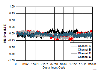
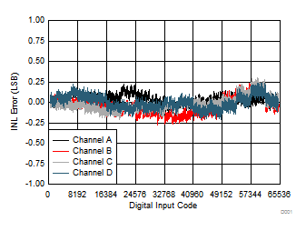
| DAC load 5 kΩ//200 pF |
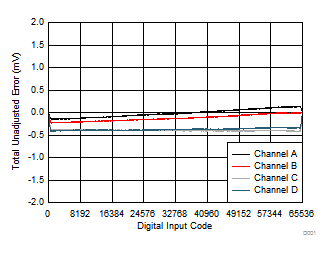
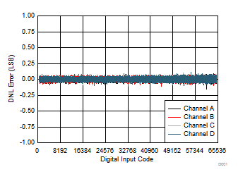
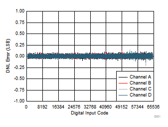
| DAC load 5 kΩ//200 pF |
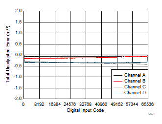
| DAC load 5 kΩ//200 pF |
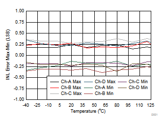
| DAC load 5 kΩ//200 pF |
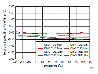
| DAC load 5 kΩ//200 pF |
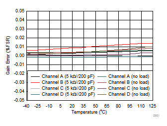
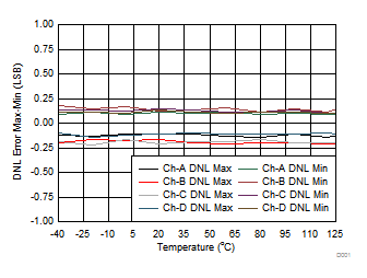
| DAC load 5 kΩ//200 pF |
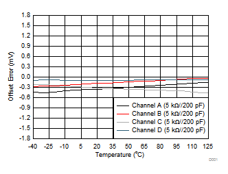
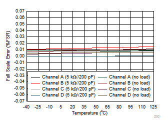
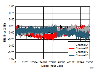
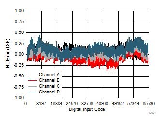
| DAC load 5 kΩ//200 pF |
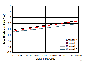
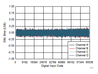
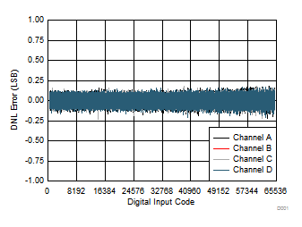
| DAC load 5 kΩ//200 pF |
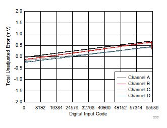
| DAC load 5 kΩ//200 pF |
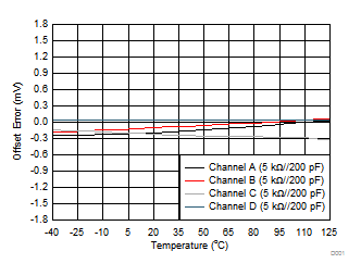
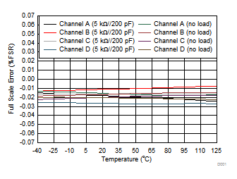
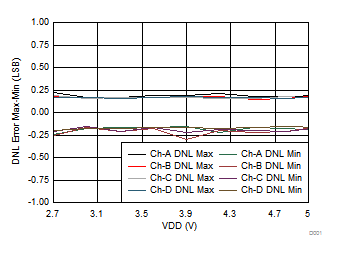
| DAC load 5 kΩ//200 pF |
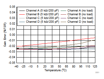
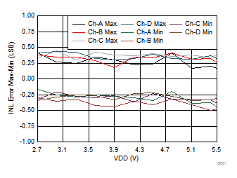
| DAC load 5 kΩ//200 pF |
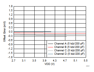
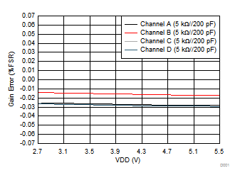
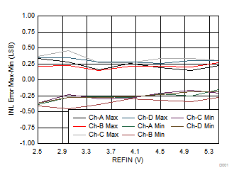
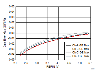
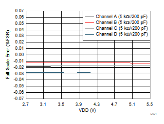
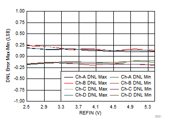
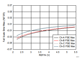

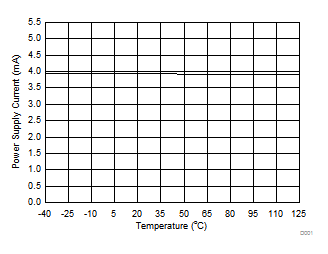
| DAC code = mid-scale code |
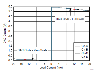
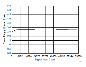
| VDD = 2.7 V, REFIN = 2.5 V |
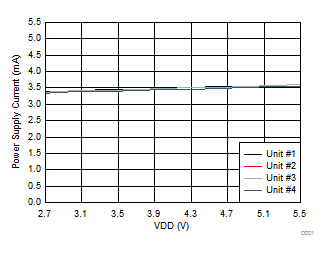
| REFIN = 2.5 V, DAC code = mid-scale code |
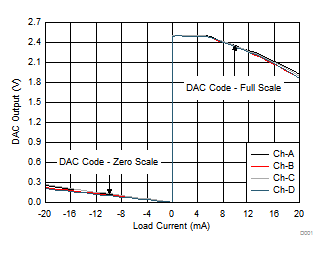
| VDD = 2.7 V, REFIN = 2.5 V |
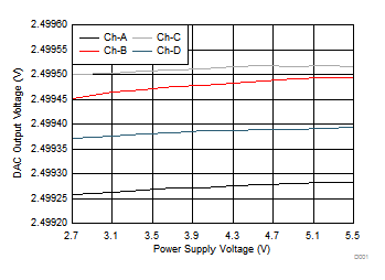
| REFIN = 2.5 V, All channels active with full-scale code, DAC unloaded |
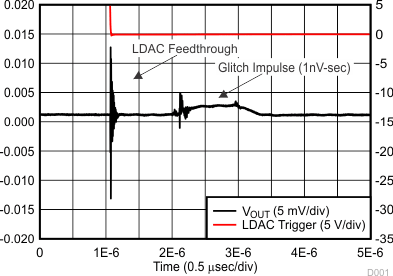
| DAC code transition from 8000h to 7FFFh |
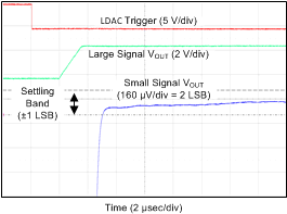
| From code 512d to 65024d, Typical channel shown |
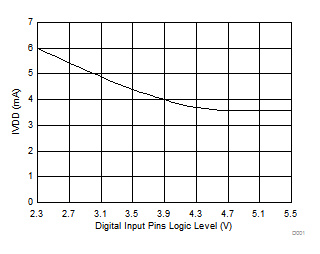
| DAC unloaded, All channels to mid-scale | ||
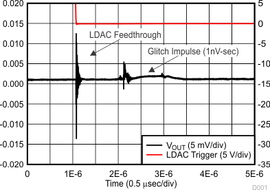
| DAC code transition from 7FFFh to 8000h |
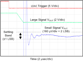
| From code 65024d to 512d, Typical channel shown |
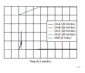
| DAC unloaded |
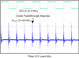
| DAC unloaded, DAC code mid-scale, Typical channel shown | ||
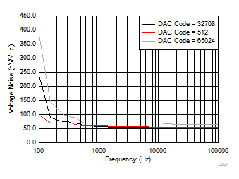
| DAC unloaded, Typical channel shown |
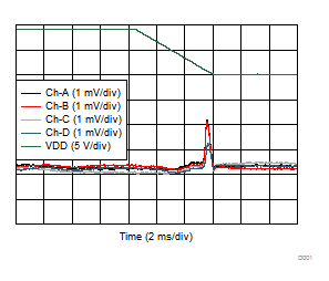
| DAC in power down mode (1 kΩ-GND) |
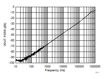
| VDD = 5.0 + 1 VPP (Sinusoid), REFIN = 2.5 V, DAC code full-scale, Typical channel shown |
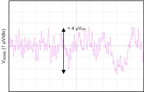
| DAC unloaded, DAC code mid-scale, Typical channel shown | ||
