ZHCSCG7B January 2014 – May 2014 DAC37J82 , DAC38J82
PRODUCTION DATA.
- 1 特性
- 2 应用范围
- 3 说明
- 4 修订历史记录
- 5 Pin Configuration and Functions
-
6 Specifications
- 6.1 Absolute Maximum Ratings
- 6.2 Handling Ratings
- 6.3 Recommended Operating Conditions
- 6.4 Thermal Information
- 6.5 DC Electrical Characteristics
- 6.6 Digital Electrical Characteristics
- 6.7 AC Electrical Characteristics
- 6.8 Timing Requirements
- 6.9 Switching Characteristics
- 6.10 Typical Characteristics
-
7 Detailed Description
- 7.1 Overview
- 7.2 Functional Block Diagram
- 7.3
Feature Description
- 7.3.1 Serdes Input
- 7.3.2 Serdes Rate
- 7.3.3 Serdes PLL
- 7.3.4 Serdes Equalizer
- 7.3.5 JESD204B Descrambler
- 7.3.6 JESD204B Frame Assembly
- 7.3.7 Serial Peripheral Interface (SPI)
- 7.3.8 Multi-Device Synchronization
- 7.3.9 Input Multiplexer
- 7.3.10 FIR Filters
- 7.3.11 Full Complex Mixer
- 7.3.12 Coarse Mixer
- 7.3.13 Dithering
- 7.3.14 Complex Summation
- 7.3.15 Quadrature Modulation Correction (QMC)
- 7.3.16 Group Delay Correction Block
- 7.3.17 Output Multiplexer
- 7.3.18 Power Measurement And Power Amplifier Protection
- 7.3.19 Serdes Test Modes
- 7.3.20 Error Counter
- 7.3.21 Eye Scan
- 7.3.22 JESD204B Pattern Test
- 7.3.23 Temperature Sensor
- 7.3.24 Alarm Monitoring
- 7.3.25 LVPECL Inputs
- 7.3.26 CMOS Digital Inputs
- 7.3.27 Reference Operation
- 7.3.28 Analog Outputs
- 7.3.29 DAC Transfer Function
- 7.4 Device Functional Modes
- 7.5 Register Map
- 8 Applications and Implementation
- 9 Power Supply Recommendations
- 10Layout
- 11器件和文档支持
- 12机械封装和可订购信息
8 Applications and Implementation
8.1 Application Information
The DAC37J82/DAC38J82 family is a 16-bit DAC with max input data rate up to 1.23GSPS per DAC. It provides one transmit paths with up to 1GHz complex information bandwidth. The DAC37J82/DAC38J82 consumes about 0.9W at 1.6GSPS and 1.1W at 2.5GSPS. The digital Quadrature Modulator Correction and Group Delay Correction enable complete IQ compensation for gain, offset, phase, and group delay between channels in direct up-conversion applications. The DAC37J82 and DAC38J82 provide the bandwidth, performance, small footprint and low power consumption needed for multi-mode 2G/3G/4G cellular base stations to migrate to more advanced technologies, such as LTE-Advanced and carrier aggregation on multiple antennas.
8.2 Typical Applications
8.2.1 Low-IF Wideband LTE Transmitter
Figure 81 shows an example block diagram for a direct conversion radio. Here it has been assumed that the desired output bandwidth is 80-MHz which could be, for instance, four 20-MHz LTE signals. It is also assumed that digital pre-distortion (DPD) is used to correct 3rd order distortion so the total DAC output bandwidth is 240 MHz. Interpolation is used to output the signal at the highest sampling rate possible to simplify the analog filtering requirements and move high order harmonics out of band. The internal PLL is used to generate the final DAC output clock from a reference clock of 307.2 MHz. The complex mixer will be used to place the baseband input signal at a desired intermediate frequency (IF). The maximum serdes rate that the chosen FPGA supports is 12.5 Gbps and the minimum number of serdes lanes is desired.
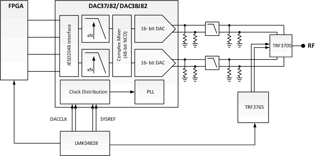 Figure 81. Low-IF Wideband LTE Transmitter Diagram
8.2.1.1 Design Requirements
For this design example, use the parameters listed in the table below as the input parameters.
| DESIGN PARAMETER | EXAMPLE VALUE |
|---|---|
| Signal Bandwidth (BWsignal) | 80 MHz |
| Total DAC Output Bandwidth (BWtotal) | 240 MHz |
| DAC PLL | On |
| DAC PLL Reference Frequency | 307.2 MHz |
| Maximum FPGA Serdes Data Rate | 12.5 Gbps |
8.2.1.2 Detailed Design Procedure
8.2.1.2.1 Data Input Rate
Nyquist theory says that the data rate must be at least two times the highest signal frequency. The data will be sent to the DAC as complex baseband data. For 240 MHz of signal bandwidth only 120 MHz of input bandwidth is needed, setting the minimum data input rate as 240 MSPS. Further, the process of interpolation requires low pass filters that limit the useable input bandwidth to about 40 percent of Fdata. Therefore, the minimum data input rate is 300 MSPS. The standard telecom data rate of 307.2 MSPS is chosen.
8.2.1.2.2 Intermediate Frequency
The intermediate frequency is chosen to keep low order harmonics out of band while staying low enough to not degrade the ACPR performance. The band of interest is 240 MHz wide, while the signal bandwidth is 80 MHz wide. The lowest frequency that the second harmonic of the signal will fall at is given on the left side of the inequality shown below based on the chosen IF center frequency. The highest frequency in the band of interest (Total DAC Output Bandwidth) is the right side of the inequality. Solving the inequality for IF and choosing a center frequency higher than that will keep the second harmonic out of the bandwidth of interest.
The lowest IF that satisfies the inequality is shown below.
So for a signal bandwidth of 80 MHz and a total bandwidth of 240 MHz, the lowest IF that satisfies the inequality is 200 MHz. Choose 220 MHz to move HD2 slightly away from the band. The full complex mixer can be enabled with the NCO frequency chosen as 220 MHz to realize this IF frequency.
8.2.1.2.3 Interpolation
It is desired to use the highest DAC output rate as possible to move the DAC images further from the signal of interest to ease the analog filter requirements. The DAC output rate must be greater than two times the highest output frequency, in this case 2 * (220 MHz + BWtotal/2) = 680 MHz. The table below shows the possible DAC output rates based on the data input rate and available interpolation settings. The DAC image frequency is also listed. Based on the result, 8x interpolation will push the image frequency 1777.6 MHz away from the band of interest, so the DAC output rate is chosen as 2457.6 MSPS.
Although not shown the high output rate also pushes higher order harmonics out of the band of interest that would have aliased back in at 1228.8 MSPS.
| INTERPOLATION | DAC OUTPUT RATE | POSSIBLE? | LOWEST IMAGE FREQUENCY | DISTANCE FROM BAND OF INTEREST |
|---|---|---|---|---|
| 1 | 307.2 MSPS | No | N/A | N/A |
| 2 | 614.4 MSPS | No | N/A | N/A |
| 4 | 1228.8 MSPS | Yes | 888.8 MHz | 548.8 MHz |
| 8 | 2457.6 MSPS | Yes | 2117.6 MHz | 1777.6 MHz |
| 16 | 4915.2 MSPS | No | N/A | N/A |
8.2.1.2.4 DAC PLL Setup
The reference frequency from an onboard clock chip, like the LMK04828, is 307.2 MHz. It is desired to use the highest PFD update rate to maintain the best phase noise performance, but not too high to avoid spurs, therefore the N Divider is chosen to be 2 for a PFD frequency of 153.6 MHz. In order to have the feedback side of the PFD be equal to the reference side (153.6 MHz) and create a DACCLK rate of 2457.6 MHz, the M Divider must be set to 16. Using Table 29, it is found that a VCO frequency of 4915.2 MHz can be used to generate a DACCLK frequency of 2457.6 MHz, so the Prescalar is set to 2 and the H-band VCO is selected.
8.2.1.2.5 Serdes Lanes
It is desired to use the minimum number of serdes lanes while staying under the maximum serdes line rate possible with the chosen FPGA. In the design requirements, the FPGA maximum serdes data rate was given as 12.5 Gbps. For the chosen input data rate of 307.2 MSPS and with 8b/10b encoding on the serdes lanes, each DAC requires a serialized data rate of 6144 Mbps, as given by the equation below.
The total serialized data rate with a dual DAC is 6144 Mbps * 2 = 12.288 Gbps. This total serialized data rate is split among the total number of lanes. The table below shows the line rate versus the total number of lanes. One lanes running at 12.288 Gbps is chosen since the minimum number of lanes is desired. This sets the JESD204B mode (LMF) for the DAC as 124 mode.
| NUMBER OF LANES | LINE RATE | POSSIBLE? |
|---|---|---|
| 1 | 12.288 Gbps | Yes |
| 2 | 6.144 Gbps | Yes |
| 4 | 3.072 Gbps | Yes |
| 8 | 1.536 Gbps | Yes |
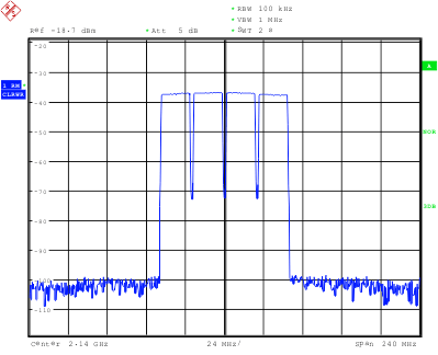
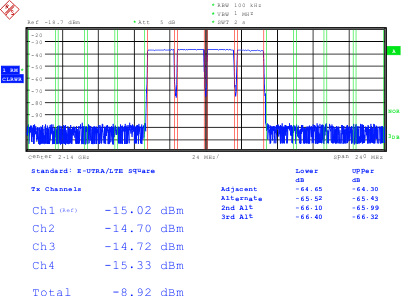
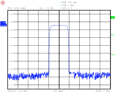
8.2.1.3 Application Performance Plots
8.2.2 Zero-IF Wideband Transmitter
The block diagram shown in Figure 84 also applies for a zero-IF wideband transmitter. However in this case the signal bandwidth is 192 MHz and digital predistortion is used to correct third and fifth order distortion, meaning the total bandwidth of interest is 960 MHz. Interpolation is used to output the signal at the highest sampling rate possible to simplify the analog filtering requirements. The DAC sample clock is provided directly from a clock chip, such as TI’s LMK04828. The maximum serdes rate that the chosen FPGA supports is 12.5 Gbps and the minimum number of serdes lanes is desired.
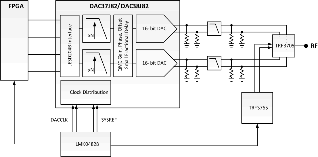 Figure 84. Zero-IF Wideband Transmitter Diagram
8.2.2.1 Design Requirements
For this design example, use the parameters listed in the table below as the input parameters.
| DESIGN PARAMETER | EXAMPLE VALUE |
|---|---|
| Signal Bandwidth (BWsignal) | 192 MHz |
| Total DAC Output Bandwidth (BWtotal) | 960 MHz |
| DAC PLL | Off |
| Maximum FPGA Serdes Data Rate | 12.5 Gbps |
8.2.2.2 Detailed Design Procedure
8.2.2.2.1 Data Input Rate
In this application the total complex bandwidth is 960 MHz meaning that at least 480 MHz of real bandwidth is needed, setting the minimum data input rate at 960 MSPS. However, the process of interpolation requires digital low pass filters that limit the useable input bandwidth to about 40 percent of Fdata. Therefore, the minimum data input rate is 1.2 GSPS.
8.2.2.2.2 Interpolation
It is desired to use the highest DAC output rate as possible to move the DAC images further from the signal of interest to ease the analog filter requirements. The DAC output rate must be greater than two times the highest output frequency, in this case 2 * 960 MHz / 2 = 960 MHz. The table below shows the possible DAC output rates based on the data input rate and available interpolation settings. The DAC image frequency is also listed. Based on the result, 2x interpolation is chosen which will push the image frequency 1.44 GHz away from the band of interest.
| INTERPOLATION | DAC OUTPUT RATE | POSSIBLE? | LOWEST IMAGE FREQUENCY | DISTANCE FROM BAND OF INTEREST |
|---|---|---|---|---|
| 1 | 1.2 GSPS | Yes | 720 MHz | 240 MHz |
| 2 | 2.4 GSPS | Yes | 1920 MHz | 1440 MHz |
| 4 | 4.8 GSPS | No | N/A | N/A |
| 8 | 9.6 GSPS | No | N/A | N/A |
| 16 | 19.2 GSPS | No | N/A | N/A |
8.2.2.2.3 Serdes Lanes
It is desired to use the minimum number of serdes lanes while staying under the maximum serdes line rate possible with the chosen FPGA. In the design requirements, the FPGA maximum serdes data rate was given as 12.5 Gbps. For the chosen input data rate of 1.2 GSPS and with 8b/10b encoding on the serdes lanes, each DAC requires a serialized data rate of 24 Gbps, as given by the equation below.
The total serialized data rate with a quad DAC is 24 Gbps * 2 = 48 Gbps. This total serialized data rate is split among the total number of lanes. The table below shows the line rate versus the total number of lanes. Four lanes must be chosen to support this data rate. This sets the JESD204B mode (LMF) for the DAC as 421 mode.
| NUMBER OF LANES | LINE RATE | POSSIBLE? |
|---|---|---|
| 1 | 48 Gbps | No |
| 2 | 24 Gbps | No |
| 4 | 12 Gbps | Yes |
| 8 | 6 Gbps | Yes |
8.2.2.2.4 LO Feedthrough and Sideband Correction
Although the I/Q modulation process will inherently reduce the level of the RF sideband signal, a zero-IF system will likely need additional sideband suppression to maximize performance. Further, any mixing process will result in some feedthrough of the LO source. The DAC37J82 and DAC38J82 contain digital features to cancel both the LO feedthrough and sideband signal. The LO feedthrough is corrected by adding a DC offset to the DAC outputs until the LO feedthrough is suppressed. The sideband suppression can be improved by correcting gain, phase, and group delay differences between the I and Q analog outputs. The phase and gain adjustments are made using the QMC block of the DAC while the group delay adjustments are done using the small fractional delay filter. First the phase should be adjusted to suppress the sideband signal at low DAC output frequencies due to phase error. Then the gain can be adjusted to further improve the suppression. Finally, the small fractional filter can be used to improve the sideband suppression across the rest of the signal bandwidth.
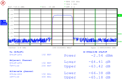
8.2.2.3 Application Performance Plots
8.3 Initialization Set Up
The following start up sequence is recommended to power up the DAC38J82/DAC37J82 family.
- Set TXENABLE low.
- Supply all 0.9-V supplies (VDDDIG09, VDDT09, VDDDAC09, VDDCLK09), all 1.8-V supplies (VDDR18, VDDS18, VQPS18, VDDIO18, VDDAPLL18, VDDAREF18), and all 3.3-V supplies (VDDADAC33). The supplies can be powered up simultaneously or in any order. There are no specific requirements on the ramp rate for the supplies.
- RESET the JTAG port by either toggling TRSTB low if using the JTAG port or holding TRSTB low if not using JTAG.
- Start the DACCLK generation.
- Toggle RESETB low to reset the SIF registers.
- Program the DAC PLL settings (config26, config49, config50, config51). If the PLL is not used, set pll_sleep and pll_reset to “1” and pll_ena to “0”.
- Program the SERDES settings (config61, config62) including the serdes_clk_sel and serdes_refclk_div.
- Program the SERDES lane settings (config63, config71, config73, config74, config96).
- Program clkjesd_div, cdrvser_sysref_mode, and interp.
- Program the JESD settings (config3, config74-77, config79, config80-85, config92, config97).
- Program the DIG block settings (NCO, PA protection, QMC, fractional delay, etc.) and set the preferred SYNC modes for the digital blocks (config30-32).
- Verify the SERDES PLL lock status by checking the SERDES PLL alarms: alarm_rw0_pll (alarm for lanes 0 through 3) and alarm_rw1_pll (alarm for lanes 4 through 7).
- Set init_state to “0000” and jesd_reset_n to “1” to start the JESD204B link initialization.
- Start the SYSREF generation.
- Enable transmission of data by asserting the TXENABLE pin or setting sif_txenable to “1”.
- Clear the alarms, then wait approximately 1-2µs and check values.
- Verify that DAC output is the desired output.