ZHCSCG7B January 2014 – May 2014 DAC37J82 , DAC38J82
PRODUCTION DATA.
- 1 特性
- 2 应用范围
- 3 说明
- 4 修订历史记录
- 5 Pin Configuration and Functions
-
6 Specifications
- 6.1 Absolute Maximum Ratings
- 6.2 Handling Ratings
- 6.3 Recommended Operating Conditions
- 6.4 Thermal Information
- 6.5 DC Electrical Characteristics
- 6.6 Digital Electrical Characteristics
- 6.7 AC Electrical Characteristics
- 6.8 Timing Requirements
- 6.9 Switching Characteristics
- 6.10 Typical Characteristics
-
7 Detailed Description
- 7.1 Overview
- 7.2 Functional Block Diagram
- 7.3
Feature Description
- 7.3.1 Serdes Input
- 7.3.2 Serdes Rate
- 7.3.3 Serdes PLL
- 7.3.4 Serdes Equalizer
- 7.3.5 JESD204B Descrambler
- 7.3.6 JESD204B Frame Assembly
- 7.3.7 Serial Peripheral Interface (SPI)
- 7.3.8 Multi-Device Synchronization
- 7.3.9 Input Multiplexer
- 7.3.10 FIR Filters
- 7.3.11 Full Complex Mixer
- 7.3.12 Coarse Mixer
- 7.3.13 Dithering
- 7.3.14 Complex Summation
- 7.3.15 Quadrature Modulation Correction (QMC)
- 7.3.16 Group Delay Correction Block
- 7.3.17 Output Multiplexer
- 7.3.18 Power Measurement And Power Amplifier Protection
- 7.3.19 Serdes Test Modes
- 7.3.20 Error Counter
- 7.3.21 Eye Scan
- 7.3.22 JESD204B Pattern Test
- 7.3.23 Temperature Sensor
- 7.3.24 Alarm Monitoring
- 7.3.25 LVPECL Inputs
- 7.3.26 CMOS Digital Inputs
- 7.3.27 Reference Operation
- 7.3.28 Analog Outputs
- 7.3.29 DAC Transfer Function
- 7.4 Device Functional Modes
- 7.5 Register Map
- 8 Applications and Implementation
- 9 Power Supply Recommendations
- 10Layout
- 11器件和文档支持
- 12机械封装和可订购信息
10 Layout
10.1 Layout Guidelines
- DAC output termination resistors should be placed as close to the output pins as possible to provide a DC path to ground and set the source impedance.
- For PLL mode, if the external loop filter is not used then leave the pin floating without any board routing. Signals coupling to this node may cause clock mixing spurs in the DAC output.
- Route the high speed serdes lanes as impedance-controlled, tightly-coupled, differential traces.
- Maintain a solid ground plane under the serdes lanes without any ground plane splits.
- AC couple the serdes lines between the logic device and the DAC using 0201 size capacitors that maintain low impedance at the serialized data rate.
- Simulation of the serdes channel is recommended to verify JESD204B standard compliance to ensure compatibility between devices.
- Keep the SYSREF routing away from the DACCLK routing to reduce coupling. Using a pulsed SYSREF or disabling a continuous SYSREF is recommended during normal operation to avoid spurs in the output spectrum.
- Keep routing for RBIAS short, for instance a resistor can be placed on the bottom of the board directly connecting the RBIAS ball to a GND ball.
- Decoupling capacitors should be placed as close to the supply pins as possible, for instance a capacitor can be placed on the bottom of the board directly connecting the supply ball to a GND ball.
- Noisy power supplies should be routed away from clean supplies. Use two power plane layers, preferably with a GND layer in between.
10.2 Layout Examples
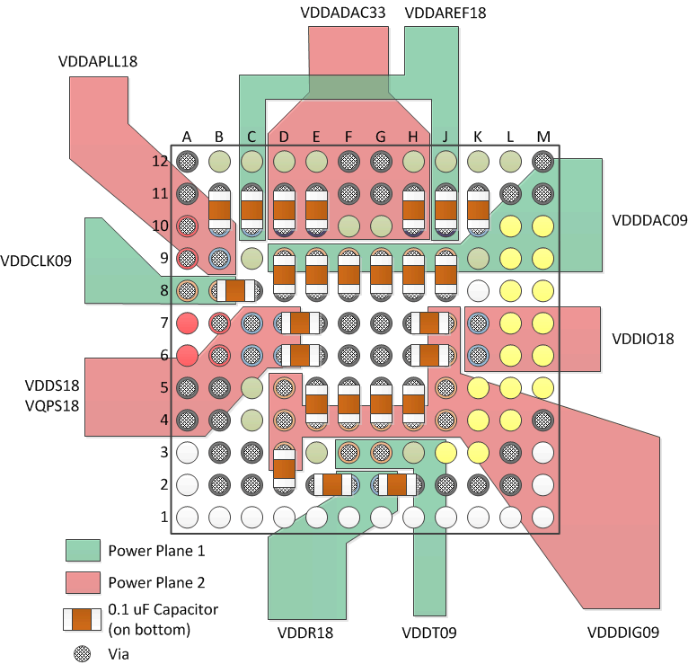 Figure 87. DAC37J82/DAC38J82 Layout for Power Supplies
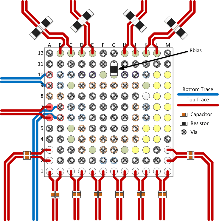 Figure 88. DAC37J82/DAC38J82 Layout for Signals