SLAS693C March   2010  – March  2015 DAC3283

PRODUCTION DATA.  

  1. Features
  2. Applications
  3. Description
  4. Simplified Schematic
  5. Revision History
  6. Pin Configuration and Functions
  7. Specifications
    1. 7.1 Absolute Maximum Ratings
    2. 7.2 ESD Ratings
    3. 7.3 Recommended Operating Conditions
    4. 7.4 Thermal Information
    5. 7.5 Electrical Characteristics - DC Specifications
    6. 7.6 Electrical Characteristics - AC Specifications
    7. 7.7 Electrical Characteristics - Digital Specifications
    8. 7.8 Timing Requirements
    9. 7.9 Typical Characteristics
  8. Detailed Description
    1. 8.1 Overview
    2. 8.2 Functional Block Diagram
    3. 8.3 Feature Description
      1. 8.3.1 Definition Of Specifications
        1. 8.3.1.1  Adjacent Carrier Leakage Ratio (ACLR)
        2. 8.3.1.2  Analog and Digital Power Supply Rejection Ratio (APSSR, DPSSR)
        3. 8.3.1.3  Differential Nonlinearity (DNL)
        4. 8.3.1.4  Gain Drift
        5. 8.3.1.5  Gain Error
        6. 8.3.1.6  Integral Nonlinearity (INL)
        7. 8.3.1.7  Intermodulation Distortion (IMD3, IMD)
        8. 8.3.1.8  Offset Drift
        9. 8.3.1.9  Offset Error
        10. 8.3.1.10 Output Compliance Range
        11. 8.3.1.11 Reference Voltage Drift
        12. 8.3.1.12 Spurious Free Dynamic Range (SFDR)
        13. 8.3.1.13 Noise Spectral Density (NSD)
    4. 8.4 Device Functional Modes
      1. 8.4.1  Serial Interface
      2. 8.4.2  Data Interface
      3. 8.4.3  Input FIFO
      4. 8.4.4  FIFO Alarms
      5. 8.4.5  FIFO Modes of Operation
        1. 8.4.5.1 Dual Sync Souces Mode
        2. 8.4.5.2 Single Sync Source Mode
        3. 8.4.5.3 Bypass Mode
      6. 8.4.6  Multi-Device Operation
        1. 8.4.6.1 Multi-Device Synchronization: Dual Sync Sources Mode
        2. 8.4.6.2 Multi-Device Operation: Single Sync Source Mode
      7. 8.4.7  Data Pattern Checker
      8. 8.4.8  DATACLK Monitor
      9. 8.4.9  FIR Filters
      10. 8.4.10 Coarse Mixer
      11. 8.4.11 Quadrature Modulation Correction (QMC)
      12. 8.4.12 Digital Offset Control
      13. 8.4.13 Temperature Sensor
      14. 8.4.14 Sleep Modes
      15. 8.4.15 LVPECL Inputs
      16. 8.4.16 LVDS INPUTS
      17. 8.4.17 CMOS Digital Inputs
      18. 8.4.18 Reference Operation
      19. 8.4.19 DAC Transfer Function
      20. 8.4.20 Analog Current Outputs
      21. 8.4.21 Passive Interface to Analog Quadrature Modulators
    5. 8.5 Register Maps
      1. 8.5.1  CONFIG0 (address = 0x00) [reset = 0x70]
      2. 8.5.2  CONFIG1 (address = 0x01) [reset = 0x11]
      3. 8.5.3  CONFIG2 (address = 0x02) [reset = 0x00]
      4. 8.5.4  CONFIG3 (address = 0x03) [reset = 0x10]
      5. 8.5.5  CONFIG4 (address = 0x04) [reset = 0xFF]
      6. 8.5.6  CONFIG5 (address = 0x05) READ ONLY
      7. 8.5.7  CONFIG6 (address =0x06) [reset = 0x00]
      8. 8.5.8  CONFIG7 (address = 0x07) [reset = 0x00] (WRITE TO CLEAR)
      9. 8.5.9  CONFIG8 (address = 0x08) [reset = 0x00] (WRITE TO CLEAR)
      10. 8.5.10 CONFIG9 (address = 0x09) [reset = 0x7A]
      11. 8.5.11 CONFIG10 (address = 0x0A) [reset = 0xB6]
      12. 8.5.12 CONFIG11 (address = 0x0B) [reset = 0xEA]
      13. 8.5.13 CONFIG12 (address =0x0C) [reset = 0x45]
      14. 8.5.14 CONFIG13 (address =0x0D) [reset = 0x1A]
      15. 8.5.15 CONFIG14 Register Name (address = 0x0E) [reset = 0x16]
      16. 8.5.16 CONFIG15 Register Name (address = 0x0F) [reset = 0xAA]
      17. 8.5.17 CONFIG16 (address = 0x10) [reset = 0xV6]
      18. 8.5.18 CONFIG17 (address = 0x11) [reset = 0x24]
      19. 8.5.19 CONFIG18 (address = 0x12) [reset = 0x02]
      20. 8.5.20 CONFIG19 (address = 0x13) [reset = 0x00]
      21. 8.5.21 CONFIG20 (address = 0x14) [reset = 0x00] (CAUSES AUTOSYNC)
      22. 8.5.22 CONFIG21 (address = 0x15) [reset = 0x00]
      23. 8.5.23 CONFIG22 (address = 0x16) [reset = 0x00]
      24. 8.5.24 CONFIG23 (address = 0x17) [reset = 0x00]
      25. 8.5.25 CONFIG24 (address = 0x18) [reset = 0x83]
      26. 8.5.26 CONFIG25 (address = 0x19) [reset = 0x00]
      27. 8.5.27 CONFIG26 (address = 0x1a) [reset = 0x00]
      28. 8.5.28 CONFIG27 (address =0x1b) [reset = 0x00] (CAUSES AUTOSYNC)
      29. 8.5.29 CONFIG28 (address = 0x1C) [reset = 0x00]
      30. 8.5.30 CONFIG29 (address = 0x1D) [reset = 0x00]
      31. 8.5.31 CONFIG30 (address = 0x1E) [reset = 0x24]
      32. 8.5.32 VERSION31 (address = 0x1F) [reset = 0x12] (PARTIAL READ ONLY)
  9. Application and Implementation
    1. 9.1 Application Information
    2. 9.2 Typical Application
      1. 9.2.1 Design Requirements
      2. 9.2.2 Detailed Design Procedure
        1. 9.2.2.1 Direct Conversion Radio
      3. 9.2.3 Application Performance Plots
  10. 10Power Supply Recommendations
    1. 10.1 Power-up Sequence
  11. 11Layout
    1. 11.1 Layout Guidelines
    2. 11.2 Layout Example
  12. 12Device and Documentation Support
    1. 12.1 Documentation Support
    2. 12.2 Trademarks
    3. 12.3 Electrostatic Discharge Caution
    4. 12.4 Glossary
  13. 13Mechanical, Packaging, and Orderable Information

封装选项

机械数据 (封装 | 引脚)
散热焊盘机械数据 (封装 | 引脚)
订购信息

6 Pin Configuration and Functions

RGZ (VQFN) Package
(Top View)
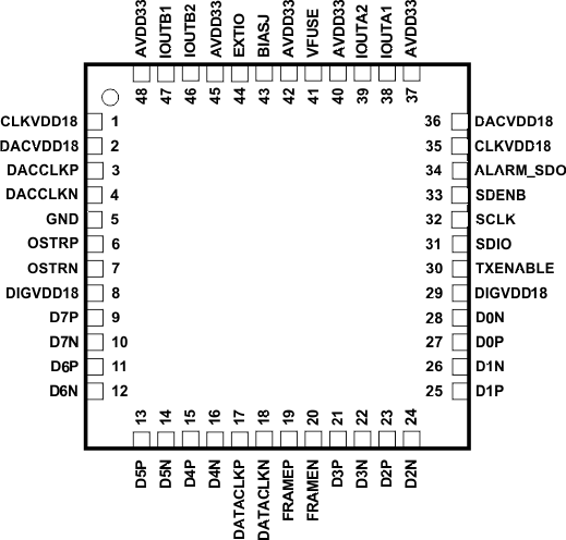
DAC3283 po_las693.gif

Pin Functions

PIN I/O DESCRIPTION
NAME NO.
AVDD33 37, 40, 42, 45, 48 I Analog supply voltage. (3.3 V)
ALARM_SDO 34 O 1.8V CMOS output for ALARM condition. The ALARM output functionality is defined through the CONFIG6 register. Default polarity is active low, but can be changed to active high via CONFIG0 alarm_pol control bit. Optionally, it can be used as the uni-directional data output in 4-pin serial interface mode (CONFIG 23 sif4_ena = '1').
BIASJ 43 O Full-scale output current bias. For 20mA full-scale output current, connect a 960Ω resistor to GND.
CLKVDD18 1, 35 I Internal clock buffer supply voltage. (1.8 V) It is recommended to isolate this supply from DACVDD18 and DIGVDD18.
D[7..0]P 9, 11, 13, 15, 21, 23, 25, 27 I LVDS positive input data bits 0 through 7. Each positive/negative LVDS pair has an internal 100 Ω termination resistor. Data format relative to DATACLKP/N clock is Double Data Rate (DDR) with two data transfers per DATACKP/N clock cycle. Dual channel 16-bit data is transferred byte-wide on this single 8-bit data bus using FRAMEP/N as a frame strobe indicator.
D7P is most significant data bit (MSB) – pin 9
D0P is least significant data bit (LSB) – pin 27
The order of the bus can be reversed via CONFIG19 rev bit.
D[7..0]N 10, 12, 14, 16, 22, 24, 26, 28 I LVDS negative input data bits 0 through 15. (See D[7:0]P description above)
D7N is most significant data bit (MSB) – pin 10
D0N is least significant data bit (LSB) – pin 28
DACCLKP 3 I Positive external LVPECL clock input for DAC core with a self-bias of approximately CLKVDD18/2.
DACCLKN 4 I Complementary external LVPECL clock input for DAC core. (see the DACCLKP description)
DACVDD18 2, 36 I DAC core supply voltage. (1.8 V) It is recommended to isolate this supply from CLKVDD18 and DIGVDD18.
DATACLKP 17 I LVDS positive input data clock. This positive/negative pair has an internal 100 Ω termination resistor. Input data D[7:0]P/N is latched on both edges of DATACLKP/N (Double Data Rate) with two data transfers input per DATACLKP/N clock cycle.
DATACLKN 18 I LVDS negative input data clock. (See DATACLKP description)
DIGVDD18 8, 29 I Digital supply voltage. (1.8V) It is recommended to isolate this supply from CLKVDD18 and DACVDD18.
EXTIO 44 I/O Used as external reference input when internal reference is disabled through CONFIG25 extref_ena = '1'. Used as internal reference output when CONFIG25 extref_ena = '0' (default). Requires a 0.1µF decoupling capacitor to AGND when used as reference output.
FRAMEP 19 I LVDS frame indicator positive input. This positive/negative pair has an internal 100Ω termination resistor. This signal is captured with the rising edge of DATACLKP/N and used to indicate the beginning of the frame. It is also used as a reset signal by the FIFO. The FRAMEP/N signal should be edge-aligned with D[7:0]P/N.
FRAMEN 20 I LVDS frame indicator negative input. (See the FRAMEN description)
GND 5, Thermal Pad I Pin 5 and the Thermal Pad located on the bottom of the QFN package is ground for all supplies.
IOUTA1 38 O A-Channel DAC current output. An offset binary data pattern of 0x0000 at the DAC input results in a full scale current sink and the least positive voltage on the IOUTA1 pin. Similarly, a 0xFFFF data input results in a 0 mA current sink and the most positive voltage on the IOUTA1 pin.
IOUTA2 39 O A-Channel DAC complementary current output. The IOUTA2 has the opposite behavior of the IOUTA1 described above. An input data value of 0x0000 results in a 0 mA sink and the most positive voltage on the IOUTA2 pin.
IOUTB1 47 O B-Channel DAC current output. Refer to IOUTA1 description above.
IOUTB2 46 O B-Channel DAC complementary current output. Refer to IOUTA2 description above.
OSTRP 6 I LVPECL output strobe positive input. This positive/negative pair is captured with the rising edge of DACCLKP/N. It is used to reset the clock dividers and for multiple DAC synchronization. If unused it can be left floating.
OSTRN 7 I LVPECL output strobe negative input. (See the OSTRP description)
SCLK 32 I 1.8V CMOS serial interface clock. Internal pull-down.
SDENB 33 I 1.8V CMOS active low serial data enable, always an input to the DAC3283. Internal pull-up.
SDIO 31 I/O 1.8V CMOS serial interface data. Bi-directional in both 3-pin mode (default) and 4-pin mode. Internal pull-down.
TXENABLE 30 I 1.8V CMOS active high input. TXENABLE must be high for the DATA to the DAC to be enabled. When TXENABLE is low, the digital logic section is forced to all 0, and any input data is ignored. Internal pull-down.
VFUSE 41 I Digital supply voltage. (1.8V) This supply pin is also used for factory fuse programming. Connect to DACVDD18 pins for normal operation.