ZHCSB79A August 2013 – August 2014 CSD95375Q4M
PRODUCTION DATA.
6 Specifications
6.1 Absolute Maximum Ratings (1)
TA = 25°C (unless otherwise noted)(1) Stresses above those listed in "Absolute Maximum Ratings" may cause permanent damage to the device. These are stress ratings only and functional operation of the device at these or any other conditions beyond those indicated under "Recommended Operating Conditions" is not implied. Exposure to Absolute Maximum rated conditions for extended periods may affect device reliability.
6.2 Recommended Operating Conditions
TA = 25° (unless otherwise noted)| MIN | MAX | UNIT | ||
|---|---|---|---|---|
| Gate Drive Voltage, VDD | 4.5 | 5.5 | V | |
| Input Supply Voltage, VIN | 16 | V | ||
| Continuous Output Current, IOUT | VIN = 12 V, VDD = 5 V, VOUT = 1.8 V, ƒSW = 500 kHz, LOUT = 0.29 µH(1) |
25 | A | |
| Peak Output Current, IOUT-PK(2) | 60 | A | ||
| Switching Frequency, ƒSW | CBST = 0.1 µF (min) | 2000 | kHz | |
| On Time Duty Cycle | 85% | |||
| Minimum PWM On Time | 40 | ns | ||
| Operating Temperature | –40 | 125 | °C | |
(1) Measurement made with six 10-µF (TDK C3216X5R1C106KT or equivalent) ceramic capacitors placed across VIN to PGND pins.
(2) System conditions as defined in Note 1. Peak Output Current is applied for tp = 10 ms, duty cycle ≤1%
6.3 Thermal Information
TA = 25°C (unless otherwise noted)| THERMAL METRIC | MIN | TYP | MAX | UNIT | |
|---|---|---|---|---|---|
| RθJC | Junction-to-Case Thermal Resistance (Top of package)(1) | 22.8 | °C/W | ||
| RθJB | Junction-to-Board Thermal Resistance(2) | 2.5 | |||
(1) RθJC is determined with the device mounted on a 1-inch² (6.45 -cm²), 2-oz (.071-mm thick) Cu pad on a 1.5-inches × 1.5-inches,
0.06-inch (1.52-mm) thick FR4 board.
0.06-inch (1.52-mm) thick FR4 board.
(2) RθJB value based on hottest board temperature within 1-mm of the package.
6.4 Electrical Characteristics
TA = 25°C, VDD = POR to 5.5 V (unless otherwise noted)| PARAMETER | TEST CONDITIONS | MIN | TYP | MAX | UNIT |
|---|---|---|---|---|---|
| PLOSS | |||||
| Power Loss(1) | VIN = 12 V, VDD = 5 V, VOUT = 1.8 V, IOUT = 15 A, ƒSW = 500 kHz, LOUT = 0.29 µH , TJ = 25°C |
2.2 | W | ||
| Power Loss(2) | VIN = 12 V, VDD = 5 V, VOUT = 1.8 V, IOUT = 15 A, ƒSW = 500 kHz, LOUT = 0.29 µH , TJ = 125°C |
2.6 | W | ||
| VIN | |||||
| VIN Quiescent Current, IQ | PWM=Floating, VDD = 5 V, VIN= 14.5 V | 1 | µA | ||
| VDD | |||||
| Standby Supply Current, IDD | PWM = Float, SKIP# = VDD or 0 V | 130 | µA | ||
| SKIP# = Float | 8 | µA | |||
| Operating Supply Current, IDD | PWM = 50% Duty cycle, ƒSW = 500 kHz | 6.4 | mA | ||
| POWER-ON RESET AND UNDER VOLTAGE LOCKOUT | |||||
| Power-On Reset, VDD Rising | 4.15 | V | |||
| UVLO, VDD Falling | 3.7 | V | |||
| Hysteresis | 0.2 | mV | |||
| PWM and SKIP# I/O Specifications | |||||
| Input Impedance, RI | Pull Up to VDD | 1700 | kΩ | ||
| Pull Down (to GND) | 800 | ||||
| Logic Level High, VIH | 2.65 | V | |||
| Logic Level Low, VIL | 0.6 | ||||
| Hysteresis, VIH | 0.2 | ||||
| Tri-State Voltage, VTS | 1.3 | 2 | |||
| Tri-state Activation Time (falling) PWM, tTHOLD(off1)(2) | 60 | ns | |||
| Tri-state Activation Time (rising) PWM, tTHOLD(off2)(2) | 60 | ||||
| Tri-state Activation Time (falling) SKIP#, tTSKF(2) | 1 | µs | |||
| Tri-state Activation Time (rising) SKIP#, tTSKR(2) | 1 | ||||
| Tri-state Exit Time PWM, t3RD(PWM)(2) | 100 | ns | |||
| Tri-state Exit Time SKIP#, t3RD(SKIP#)(2) | 50 | µs | |||
| BOOTSTRAP SWITCH | |||||
| Forward Voltage, VFBST | IF = 10 mA | 120 | 240 | mV | |
| Reverse Leakage, IRLEAK | VBST – VDD = 25 V | 2 | µA | ||
(1) Measurement made with six 10-µF (TDK C3216X5R1C106KT or equivalent) ceramic capacitors placed across VIN to PGND pins.
(2) Specified by design
6.5 Typical Characteristics
TJ = 125°C, unless stated otherwise.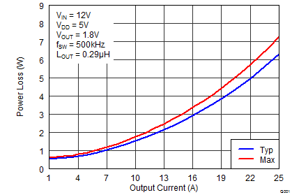
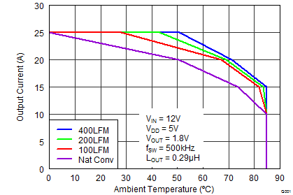
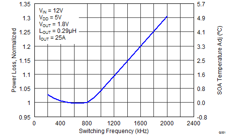
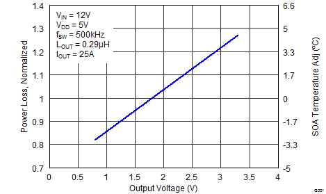
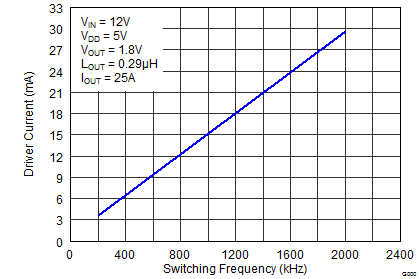
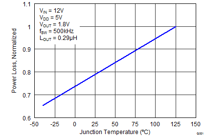
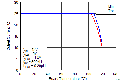

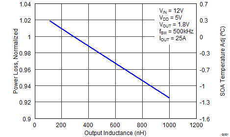
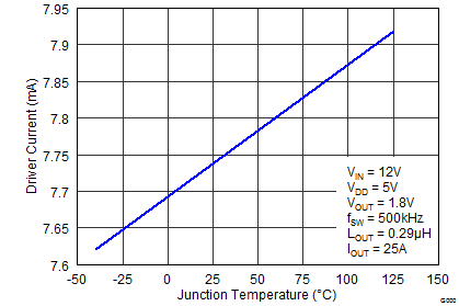
- The Typical CSD95375Q4M System Characteristic curves are based on measurements made on a PCB design with dimensions of 4" (W) × 3.5" (L) × 0.062" (T) and 6 copper layers of 1 oz. copper thickness. See the Application Information section for detailed explanation.