SCLS464A September 2002 – January 2015 CD74HC4051-EP
PRODUCTION DATA.
- 1 Features
- 2 Applications
- 3 Description
- 4 Revision History
- 5 Pin Configuration And Functions
- 6 Specifications
- 7 Parameter Measurement Information
- 8 Detailed Description
- 9 Application and Implementation
- 10Power Supply Recommendations
- 11Layout
- 12Device And Documentation Support
- 13Mechanical, Packaging, and Orderable Information
6 Specifications
6.1 Absolute Maximum Ratings
over operating free-air temperature range (unless otherwise noted) (1)| MIN | MAX | UNIT | ||
|---|---|---|---|---|
| VCC – VEE(2) | Supply voltage | –0.5 | 10.5 | V |
| VCC | –0.5 | 7 | ||
| VEE | 0.5 | –7 | ||
| IIK | Input clamp current (VI < –0.5 V or VI > VCC + 0.5 V) | –20 | 20 | mA |
| IOK | Output clamp current (VO < VEE – 0.5 V or VO > VCC + 0.5 V) | –20 | 20 | mA |
| Switch current (VI > VEE – 0.5 V or VI < VCC + 0.5 V) | –25 | 25 | mA | |
| Continuous current through VCC or GND | –50 | 50 | mA | |
| IEE | VEE current | 0 | 20 | mA |
| θJA | Package thermal impedance(3) | 73 | °C/W | |
| TJ | Maximum junction temperature | 150 | °C | |
| Tstg | Storage temperature | –65 | 150 | °C |
(1) Stresses beyond those listed under Absolute Maximum Ratings may cause permanent damage to the device. These are stress ratings only, which do not imply functional operation of the device at these or any other conditions beyond those indicated under Recommended Operating Conditions. Exposure to absolute-maximum-rated conditions for extended periods may affect device reliability.
(2) All voltages referenced to GND unless otherwise specified.
(3) The package thermal impedance is calculated in accordance with JESD 51-7.
6.2 ESD Ratings
| VALUE | UNIT | ||||
|---|---|---|---|---|---|
| V(ESD) | Electrostatic discharge | Human body model (HBM), per ANSI/ESDA/JEDEC JS-001, all pins(1) | ±2000 | V | |
| Charged device model (CDM), per JEDEC specification JESD22-C101, all pins(2) | ±500 | ||||
(1) JEDEC document JEP155 states that 500-V HBM allows safe manufacturing with a standard ESD control process.
(2) JEDEC document JEP157 states that 250-V CDM allows safe manufacturing with a standard ESD control process.
6.3 Recommended Operating Conditions(1)
over operating free-air temperature range (unless otherwise noted)| MIN | NOM | MAX | UNIT | |||
|---|---|---|---|---|---|---|
| VCC | Supply voltage(2) | 2 6 | 6 | V | ||
| Supply voltage, VCC – VEE (see Figure 4) | 2 10 | 10 | V | |||
| VEE | Supply voltage, (see (2) and Figure 5) | 0 –6 | –6 | V | ||
| VIH | High-level input voltage | VCC = 2 V | 1.5 | V | ||
| VCC = 4.5 V | 3.15 | |||||
| VCC = 6 V | 4.2 | |||||
| VIL | Low-level input voltage | VCC = 2 V | 0.5 | V | ||
| VCC = 4.5 V | 1.35 | |||||
| VCC = 6 V | 1.8 | |||||
| VI | Input control voltage | 0 | VCC | V | ||
| VIS | Analog switch I/O voltage | VEE | VCC | V | ||
| tt | Input transition (rise and fall) time | VCC = 2 V | 0 | 1000 | ns | |
| VCC = 4.5 V | 0 | 500 | ||||
| VCC = 6 V | 0 | 400 | ||||
| TA | Operating free-air temperature | –55 | 125 | °C | ||
| Cpd | Power dissipation capacitance(3) | 50 | pF | |||
(1) All unused inputs of the device must be held at VCC or GND to ensure proper device operation. Refer to the TI application report, Implications of Slow or Floating CMOS Inputs, SCBA004.
(2) In certain applications, the external load resistor current may include both VCC and signal-line components. To avoid drawing VCC current when switch current flows into the transmission gate inputs, the voltage drop across the bidirectional switch must not exceed 0.6 V (calculated from ron values shown in Electrical Characteristics table). No VCC current flows through RL if the switch current flows into the COM OUT/IN A terminal.
(3) Cpd is used to determine the dynamic power consumption, per package.
PD = Cpd VCC2 fI + Σ (CL + CS) VCC2 fO
fO = output frequency
fI = input frequency
CL = output load capacitance
CS = switch capacitance
VCC = supply voltage
PD = Cpd VCC2 fI + Σ (CL + CS) VCC2 fO
fO = output frequency
fI = input frequency
CL = output load capacitance
CS = switch capacitance
VCC = supply voltage
6.4 Thermal Information
| THERMAL METRIC(1) | CD74HC4051-EP | UNIT | |
|---|---|---|---|
| D (SOIC) | |||
| 16 PINS | |||
| RθJA | Junction-to-ambient thermal resistance | 81.7 | °C/W |
| RθJC(top) | Junction-to-case (top) thermal resistance | 43.1 | |
| RθJB | Junction-to-board thermal resistance | 39.2 | |
| ψJT | Junction-to-top characterization parameter | 10.7 | |
| ψJB | Junction-to-board characterization parameter | 38.9 | |
(1) For more information about traditional and new thermal metrics, see the IC Package Thermal Metrics application report, SPRA953.
6.5 Electrical Characteristics
over operating free-air temperature range (unless otherwise noted)| PARAMETER | TEST CONDITIONS | VEE | VCC | TA = 25°C | TA = –55°C to 125°C | UNIT | |||||
|---|---|---|---|---|---|---|---|---|---|---|---|
| MIN | TYP | MAX | MIN | TYP | MAX | ||||||
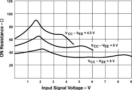
| ron | IO = 1 mA, VI = VIH or VIL, See Figure 1 |
VIS = VCC or VEE | 0 V | 4.5 V | 70 | 160 | 240 | Ω | |||
| 0 V | 6 V | 60 | 140 | 210 | |||||||
| –4.5 V | 4.5 V | 40 | 120 | 180 | |||||||
| VIS = VCC to VEE | 0 V | 4.5 V | 90 | 180 | 270 | ||||||
| 0 V | 6 V | 80 | 160 | 240 | |||||||
| –4.5 V | 4.5 V | 45 | 130 | 195 | |||||||
| ∆ron | Between any two channels | 0 V | 4.5 V | 10 | Ω | ||||||
| 0 V | 6 V | 8.5 | |||||||||
| –4.5 V | 4.5 V | 5 | |||||||||
| IIZ | For switch OFF: When VIS = VCC, VOS = VEE; When VIS = VEE, VOS = VCC For switch ON: All applicable combinations of VIS and VOS voltage levels, VI = VIH or VIL |
0 V | 6 V | ±0.2 | ±2 | µA | |||||
| –5 V | 5 V | ±0.4 | ±4 | ||||||||
| IIL | VI = VCC or GND | 0 V | 6 V | ±0.1 | ±1 | µA | |||||
| ICC | IO = 0, VI = VCC or GND | When VIS = VEE, VOS = VCC | 0 V | 6 V | 8 | 160 | µA | ||||
| When VIS = VCC, VOS = VEE | –5 V | 5 V | 16 | 320 | |||||||
6.6 Analog Channel Characteristics
TA = 25°C| PARAMETER | TEST CONDITIONS | VEE | VCC | MIN | TYP | MAX | UNIT | |
|---|---|---|---|---|---|---|---|---|
| CI | Switch input capacitance | 5 | pF | |||||
| CCOM | Common output capacitance | 25 | pF | |||||
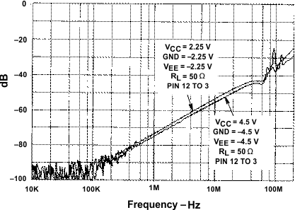
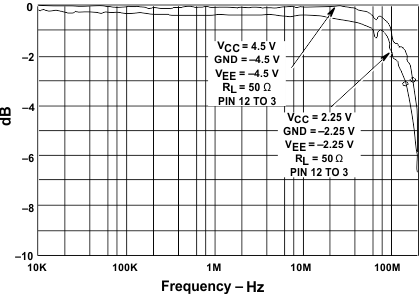
| fmax | Minimum switch frequency response at –3 dB | See Figure 6, Figure 2, and (1)(2) | –2.25 V | 2.25 V | 145 | MHz | ||
| –4.5 V | 4.5 V | 180 | ||||||
| Sine-wave distortion | See Figure 7 | –2.25 V | 2.25 V | 0.03% | ||||
| –4.5 V | 4.5 V | 0.018% | ||||||
| Switch OFF signal feedthrough | See Figure 8, Figure 3 and (2)(3) | –2.25 V | 2.25 V | –73 | dB | |||
| –4.5 V | 4.5 V | –75 | ||||||
(1) Adjust input voltage to obtain 0 dBm at VOS for fIN = 1 MHz.
(2) VIS is centered at (VCC – VEE)/2.
(3) Adjust input for 0 dBm
6.7 Switching Characteristics
over recommended operating free-air temperature range (unless otherwise noted) (see Figure 9)| PARAMETER | FROM (INPUT) |
TO (OUTPUT) |
LOAD CAPACITANCE |
VEE | VCC | TA = 25°C | TA = –55°C TO 125°C | UNIT | ||||
|---|---|---|---|---|---|---|---|---|---|---|---|---|
| MIN | TYP | MAX | MIN | TYP | MAX | |||||||
| tpd | IN | OUT | CL = 15 pF | 5 V | 4 | ns | ||||||
| CL = 50 pF | 0 V | 2 V | 60 | 90 | ||||||||
| 4.5 V | 12 | 18 | ||||||||||
| 6 V | 10 | 15 | ||||||||||
| –4.5 V | 4.5 V | 8 | 12 | |||||||||
| CL = 15 pF | 5 V | 19 | ns | |||||||||
| ten | ADDRESS SEL or E | OUT | CL = 50 pF | 0 V | 2 V | 225 | 340 | |||||
| 4.5 V | 45 | 68 | ||||||||||
| 6 V | 38 | 57 | ||||||||||
| –4.5 V | 4.5 V | 32 | 48 | |||||||||
| tdis | ADDRESS SEL or E | OUT | CL = 15 pF | 5 V | 19 | ns | ||||||
| CL = 50 pF | 0 V | 2 V | 225 | 340 | ||||||||
| 4.5 V | 45 | 68 | ||||||||||
| 6 V | 38 | 57 | ||||||||||
| –4.5 V | 4.5 V | 32 | 48 | |||||||||
| CI | Control | CL = 50 pF | 10 | 10 | pF | |||||||
6.8 Typical Characteristics
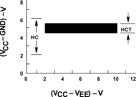
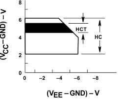
6.8.1 Recommended Operating Area as a Function of Supply Voltages