ZHCSJ35C September 2016 – May 2021 CC3220R , CC3220S , CC3220SF
PRODUCTION DATA
- 1 特性
- 2 应用
- 3 说明
- 4 功能方框图
- 5 Revision History
- 6 Device Comparison
- 7 Terminal Configuration and Functions
-
8 Specifications
- 8.1 Absolute Maximum Ratings
- 8.2 ESD Ratings
- 8.3 Power-On Hours (POH)
- 8.4 Recommended Operating Conditions
- 8.5 Current Consumption Summary (CC3220R, CC3220S)
- 8.6 Current Consumption Summary (CC3220SF)
- 8.7 TX Power and IBAT versus TX Power Level Settings
- 8.8 Brownout and Blackout Conditions
- 8.9 Electrical Characteristics (3.3 V, 25°C)
- 8.10 WLAN Receiver Characteristics
- 8.11 WLAN Transmitter Characteristics
- 8.12 WLAN Filter Requirements
- 8.13 Thermal Resistance Characteristics
- 8.14
Timing and Switching Characteristics
- 8.14.1 Power Supply Sequencing
- 8.14.2 Device Reset
- 8.14.3 Reset Timing
- 8.14.4 Wakeup From HIBERNATE Mode
- 8.14.5 Clock Specifications
- 8.14.6
Peripherals Timing
- 8.14.6.1 SPI
- 8.14.6.2 I2S
- 8.14.6.3 GPIOs
- 8.14.6.4 I2C
- 8.14.6.5 IEEE 1149.1 JTAG
- 8.14.6.6 ADC
- 8.14.6.7 Camera Parallel Port
- 8.14.6.8 UART
- 8.14.6.9 SD Host
- 8.14.6.10 Timers
- 9 Detailed Description
- 10Applications, Implementation, and Layout
- 11Device and Documentation Support
- 12Mechanical, Packaging, and Orderable Information
10.1.2 Typical Application Schematic—CC3220x Preregulated, 1.85-V Mode
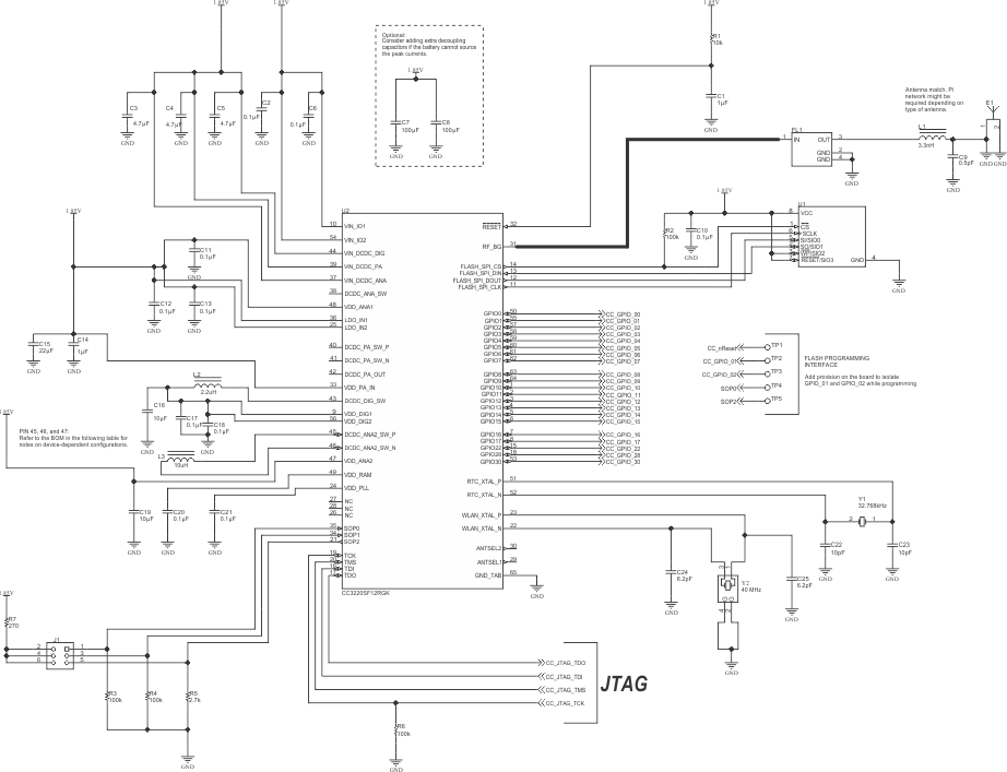
Figure 10-2 shows the typical application schematic using the CC3220x in preregulated, 1.85-V mode of operation. For addition information on this mode of operation please contact your TI representative.
 Figure 10-2 CC3220x Preregulated 1.85-V
Mode Application Circuit
Figure 10-2 CC3220x Preregulated 1.85-V
Mode Application CircuitTable 10-2 lists the bill of materials for an application using the CC3120R device in preregulated 1.85-V mode.
Table 10-2 Bill of Materials for CC3220x
Preregulated, 1.85-V Mode
| QUANTITY | DESIGNATOR | VALUE | MANUFACTURER | PART NUMBER | DESCRIPTION |
|---|---|---|---|---|---|
| 1 | C1 | 1 µF | MuRata | GRM155R61A105KE15D | Capacitor, Ceramic, 1 µF, 10 V, ±10%, X5R, 0402 |
| 10 | C2, C6, C10, C11, C12, C13, C17, C18, C20, C21 | 0.1 µF | TDK | C1005X5R1A104K050BA | Capacitor, Ceramic, 0.1 µF, 10 V, ±10%, X5R, 0402 |
| 3 | C3, C4, C5 | 4.7 µF | TDK | C1005X5R0J475M050BC | Capacitor, Ceramic, 4.7 µF, 6.3 V, ±20%, X5R, 0402 |
| 2 | C7, C8 | 100 µF | Taiyo Yuden | LMK325ABJ107MMHT | Capacitor, Ceramic, 100 µF, 10 V, ± 20%, X5R, AEC-Q200 Grade 3, 1210 |
| 1 | C9 | 0.5 pF | MuRata | GRM1555C1HR50BA01D | Capacitor, Ceramic, 0.5 pF, 50 V, ±20%, C0G/NP0, 0402 |
| 1 | C14 | 1 µF | TDK | C1005X5R1A105K050BB | Capacitor, Ceramic, 1 µF, 10 V, ±10%, X5R, 0402 |
| 1 | C15 | 22 µF | TDK | C1608X5R0G226M080AA | Capacitor, Ceramic, 22 µF, 4 V, ±20%, X5R, 0603 |
| 2 | C16, C19 | 10 µF | MuRata | GRM188R60J106ME47D | Capacitor, Ceramic, 10 µF, 6.3 V, ±20%, X5R, 0603 |
| 2 | C22, C23 | 10 pF | MuRata | GRM1555C1H100JA01D | Capacitor, Ceramic, 10 pF, 50 V, ±5%, C0G/NP0, 0402 |
| 2 | C24, C25 | 6.2 pF | MuRata | GRM1555C1H6R2CA01D | Capacitor, Ceramic, 6.2 pF, 50 V, ±5%, C0G/NP0, 0402 |
| 1 | U1 | MX25R | Macronix International Co. LTD | MX25R3235FM1IL0 | Ultra-low power, 32-Mbit [x 1/x 2/x 4] CMOS MXSMIO (Serial Multi I/O) Flash Memory, SOP-8 |
| 1 | E1 | 2.45-GHz Antenna | Taiyo Yuden | AH316M245001-T | ANT Bluetooth W-LAN Zigbee®WiMAX™, SMD |
| 1 | FL1 | 1.02 dB | TDK | DEA202450BT-1294C1-H | Multilayer Chip Band Pass Filter For 2.4GHz W-LAN/Bluetooth, SMD |
| 1 | L1 | 3.3 nH | MuRata | LQG15HS3N3S02D | Inductor, Multilayer, Air Core, 3.3 nH, 0.3 A, 0.17 ohm, SMD |
| 1 | L2 | 2.2 µH | MuRata | LQM2HPN2R2MG0L | Inductor, Multilayer, Ferrite, 2.2 µH, 1.3 A, 0.08 ohm, SMD |
| 1 | L3(1) | 10 µH | Taiyo Yuden | CBC2518T100M | Inductor, Wirewound, Ceramic, 10 µH, 0.48 A, 0.36 ohm, SMD |
| 1 | R1 | 10 k | Vishay-Dale | CRCW040210K0JNED | Resistor, 10 k, 5%, 0.063 W, 0402 |
| 4 | R2, R3, R4, R6 | 100 k | Vishay-Dale | CRCW0402100KJNED | Resistor, 100 k, 5%, 0.063 W, 0402 |
| 1 | R5 | 2.7 k | Vishay-Dale | CRCW04022K70JNED | Resistor, 2.7 k, 5%, 0.063 W, 0402 |
| 1 | R7 | 270 | Vishay-Dale | CRCW0402270RJNED | Resistor, 270, 5%, 0.063 W, 0402 |
| 1 | U2 | CC3220 | Texas Instruments | CC3220SF12RGK | SimpleLink™ Wi-Fi® and internet-of-things solution, a Single-Chip Wireless MCU, RGK0064B |
| 1 | Y1 | Crystal | Abracon Corporation | ABS07-32.768KHZ-9-T | Crystal, 32.768 kHZ, 9PF, SMD |
| 1 | Y2 | Crystal | Epson | Q24FA20H0039600 | Crystal, 40 MHz, 8pF, SMD |
(1) For CC3220SF device, L3 is
populated. For CC3220R and CC3220S devices, L3 is not populated and Pin 47 can
be used as GPIO_31.