SWRS105B May 2011 – June 2014 CC115L
PRODUCTION DATA.
- 1Device Overview
- 2Revision History
- 3Terminal Configuration and Functions
- 4Specifications
-
5Detailed Description
- 5.1 Overview
- 5.2 Functional Block Diagram
- 5.3 Configuration Overview
- 5.4 Configuration Software
- 5.5 4-wire Serial Configuration and Data Interface
- 5.6 Microcontroller Interface and Pin Configuration
- 5.7 Data Rate Programming
- 5.8 Packet Handling Hardware Support
- 5.9 Modulation Formats
- 5.10 Radio Control
- 5.11 TX FIFO
- 5.12 Frequency Programming
- 5.13 VCO
- 5.14 Voltage Regulators
- 5.15 Output Power Programming
- 5.16 General Purpose and Test Output Control Pins
- 5.17 Asynchronous and Synchronous Serial Operation
- 5.18 System Considerations and Guidelines
- 5.19 Configuration Registers
- 5.20 Development Kit Ordering Information
- 6Applications, Implementation, and Layout
- 7Device and Documentation Support
- 8Mechanical Packaging and Orderable Information
5 Detailed Description
5.1 Overview
The CC115L transmitter is based on direct synthesis of the RF frequency. The frequency synthesizer includes a completely on-chip LC VCO.
A crystal is to be connected to XOSC_Q1 and XOSC_Q2. The crystal oscillator generates the reference frequency for the synthesizer, as well as clocks for the ADC and the digital part.
A 4-wire SPI is used for configuration and data buffer access.
The digital baseband includes support for channel configuration, packet handling, and data buffering.
5.2 Functional Block Diagram
A simplified block diagram of CC115L is shown in Figure 5-1.
 Figure 5-1 CC115L Simplified Block Diagram
5.3 Configuration Overview
CC115L can be configured to achieve optimum performance for many different applications. Configuration is done using the SPI interface. See Section 5.5 for more description of the SPI interface. The following key parameters can be programmed:
- Power-down / power up mode
- Crystal oscillator power-up / power-down
- Carrier frequency / RF channel
- Transmit mode
- Data rate
- Modulation format
- RF output power
- Data buffering with separate 64-byte TX FIFO
- Packet radio hardware support
Details of each configuration register can be found in Section 5.19.
Figure 5-2 shows a simplified state diagram that explains the main CC115L states together with typical usage and current consumption. For detailed information on controlling the CC115L state machine, and a complete state diagram, see Section 5.10.
 Figure 5-2 Simplified Radio Control State Diagram with Typical Current Consumption
5.4 Configuration Software
CC115L can be configured using the SmartRF™ Studio software SWRC176. The SmartRF Studio software is highly recommended for obtaining optimum register settings, and for evaluating performance and functionality.
After chip reset, all the registers have default values as shown Section 5.19. The optimum register setting might differ from the default value. After a reset all registers that shall be different from the default value therefore needs to be programmed through the SPI interface.
5.5 4-wire Serial Configuration and Data Interface
CC115L is configured through a simple 4-wire SPI-compatible interface (SI, SO, SCLK and CSn) where CC115L is the slave. This interface is also used write buffered data. All transfers on the SPI interface are done most significant bit first.
All transactions on the SPI interface start with a header byte containing a R/W bit, a burst access bit (B), and a 6-bit address (A5–A0).
The CSn pin must be kept low during transfers on the SPI bus. If CSn goes high during the transfer of a header byte or during read/write from/to a register, the transfer will be cancelled. The timing for the address and data transfer on the SPI interface is shown in Figure 5-3 with reference to Table 5-1.
When CSn is pulled low, the MCU must wait until CC115L SO pin goes low before starting to transfer the header byte. This indicates that the crystal is running. Unless the chip was in the SLEEP or XOFF states, the SO pin will always go low immediately after taking CSn low.
 Figure 5-3 Configuration Registers Write and Read Operations
Table 5-1 SPI Interface Timing Requirements
| Parameter | Description | Min | Max | Units | |
|---|---|---|---|---|---|
| fSCLK | SCLK frequency | – | 10 | MHz | |
| 100 ns delay inserted between address byte and data byte (single access), or between address and data, and between each data byte (burst access). | |||||
| SCLK frequency, single access | – | 9 | |||
| No delay between address and data byte | |||||
| SCLK frequency, burst access | – | 6.5 | |||
| No delay between address and data byte, or between data bytes | |||||
| tsp,pd | CSn low to positive edge on SCLK, in power-down mode | 150 | – | µs | |
| tsp | CSn low to positive edge on SCLK, in active mode | 20 | – | ns | |
| tch | Clock high | 50 | – | ns | |
| tcl | Clock low | 50 | – | ns | |
| trise | Clock rise time | – | 40 | ns | |
| tfall | Clock fall time | – | 40 | ns | |
| tsd | Setup data (negative SCLK edge) to positive edge on SCLK (tsd applies between address and data bytes, and between data bytes) | Single access | 55 | – | ns |
| Burst access | 76 | – | |||
| thd | Hold data after positive edge on SCLK | 20 | – | ns | |
| tns | Negative edge on SCLK to CSn high. | 20 | – | ns | |
NOTE
The minimum tsp,pd figure in Table 5-1 can be used in cases where the user does not read the CHIP_RDYn signal. CSn low to positive edge on SCLK when the chip is woken from power-down depends on the start-up time of the crystal being used. The 150 μs in Table 5-1 is the crystal oscillator start-up time measured on SWRR046 and SWRR045 using crystal AT-41CD2 from NDK.
5.5.1 Chip Status Byte
When the header byte, data byte, or command strobe is sent on the SPI interface, the chip status byte is sent by the CC115L on the SO pin. The status byte contains key status signals, useful for the MCU. The first bit, s7, is the CHIP_RDYn signal and this signal must go low before the first positive edge of SCLK. The CHIP_RDYn signal indicates that the crystal is running.
Bits 6, 5, and 4 comprise the STATE value. This value reflects the state of the chip. The XOSC and power to the digital core are on in the IDLE state, but all other modules are in power down. The frequency and channel configuration should only be updated when the chip is in this state.
The last four bits (3:0) in the status byte contains FIFO_BYTES_AVAILABLE. For these bits to give any valid information, the R/W bit in the header byte must be set to 0. The FIFO_BYTES_AVAILABLE field contains the number of bytes that can be written to the TX FIFO. When FIFO_BYTES_AVAILABLE=15, 15 or more bytes can be written.
Table 5-2 gives a status byte summary.
Table 5-2 Status Byte Summary
| Bits | Name | Description | ||
|---|---|---|---|---|
| 7 | CHIP_RDYn | Stays high until power and crystal have stabilized. Should always be low when using the SPI interface. | ||
| 6:4 | STATE[2:0] | Indicates the current main state machine mode | ||
| Value | State | Description | ||
| 000 | IDLE | IDLE state (Also reported for some transitional states instead of SETTLING or CALIBRATE) |
||
| 001 | Reserved | |||
| 010 | TX | Transmit mode | ||
| 011 | FSTXON | Fast TX ready | ||
| 100 | CALIBRATE | Frequency synthesizer calibration is running | ||
| 101 | SETTLING | PLL is settling | ||
| 110 | Reserved | |||
| 111 | TXFIFO_UNDERFLOW | TX FIFO has underflowed. Acknowledge with SFTX | ||
| 3:0 | FIFO_BYTES_AVAILABLE[3:0] | The number of bytes that can be written to the TX FIFO | ||
5.5.2 Register Access
The configuration registers on the CC115L are located on SPI addresses from 0x00 to 0x2E. Table 5-14 lists all configuration registers. It is highly recommended to use SmartRF Studio SWRC176 to generate optimum register settings. The detailed description of each register is found in Section 5.19.1 and Section 5.19.2. All configuration registers can be both written to and read. The R/W bit controls if the register should be written to or read. When writing to registers, the status byte is sent on the SO pin each time a header byte or data byte is transmitted on the SI pin. When reading from registers, the status byte is sent on the SO pin each time a header byte is transmitted on the SI pin.
Registers with consecutive addresses can be accessed in an efficient way by setting the burst bit (B) in the header byte. The address bits (A5 - A0) set the start address in an internal address counter. This counter is incremented by one each new byte (every 8 clock pulses). The burst access is either a read or a write access and must be terminated by setting CSn high.
For register addresses in the range 0x30 - 0x3D, the burst bit is used to select between status registers when burst bit is one, and between command strobes when burst bit is zero (see Section 5.5.3). Because of this, burst access is not available for status registers and they must be accessed one at a time. The status registers can only be read.
5.5.3 SPI Read
When reading register fields over the SPI interface while the register fields are updated by the radio hardware (that is, MARCSTATE or TXBYTES), there is a small, but finite, probability that a single read from the register is being corrupt. As an example, the probability of any single read from TXBYTES being corrupt, assuming the maximum data rate is used, is approximately 80 ppm. Refer to the CC115L Errata Notes SWRZ037 for more details.
5.5.4 Command Strobes
Command Strobes may be viewed as single byte instructions to CC115L. By addressing a command strobe register, internal sequences will be started. These commands are used to disable the crystal oscillator, enable transmit mode, enable calibration etc. The 11 command strobes are listed in Table 5-13.
NOTE
An SIDLE strobe will clear all pending command strobes until IDLE state is reached. This means that if for example an SIDLE strobe is issued while the radio is in TX state, any other command strobes issued before the radio reaches IDLE state will be ignored.
The command strobe registers are accessed by transferring a single header byte (no data is being transferred). That is, only the R/W bit, the burst access bit (set to 0), and the six address bits (in the range 0x30 through 0x3D) are written. The R/W bit should be set to zero if the FIFO_BYTES_AVAILABLE field in the status byte should be interpreted.
When writing command strobes, the status byte is sent on the SO pin.
A command strobe may be followed by any other SPI access without pulling CSn high. However, if an SRES strobe is being issued, one will have to wait for SO to go low again before the next header byte can be issued as shown in Figure 5-4. The command strobes are executed immediately, with the exception of the SPWD and the SXOFF strobes, which are executed when CSn goes high.
 Figure 5-4 SRES Command Strobe
5.5.5 TX FIFO Access
The 64-byte TX FIFO is accessed through the 0x3F address. The TX FIFO is write-only and the R/W bit should therefore be zero.
The burst bit is used to determine if the TX FIFO access is a single byte access or a burst access. The single byte access method expects a header byte with the burst bit set to zero and one data byte. After the data byte, a new header byte is expected; hence CSn can remain low. The burst access method expects one header byte and then consecutive data bytes until terminating the access by setting CSn high.
The following header bytes access the FIFO:
- 0x3F: Single byte access to TX FIFO
- 0x7F: Burst access to TX FIFO
When writing to the TX FIFO, the status byte (see Section 5.5.1) is output on SO for each new data byte as shown in Figure 5-3. This status byte can be used to detect TX FIFO underflow while writing data to the TX FIFO. Note that the status byte contains the number of bytes free before writing the byte in progress to the TX FIFO. When the last byte that fits in the TX FIFO is transmitted on SI, the status byte received concurrently on SO will indicate that one byte is free in the TX FIFO.
The TX FIFO may be flushed by issuing a SFTX command strobe. A SFTX command strobe can only be issued in the IDLE, or TXFIFO_UNDERFLOW states. The TX FIFO is flushed when going to the SLEEP state.
Figure 5-5 gives a brief overview of different register access types possible.
5.5.6 PATABLE Access
The 0x3E address is used to access the PATABLE, which is used for selecting PA power control settings. The SPI expects one or two data bytes after receiving the address (the burst bit must be set if two bytes are to be written). For OOK, two bytes should be written to PATABLE; the first byte after the address will set the logic 0 power level and the second byte written will set the logic 1 power level. For all other modulations formats, only one byte should be written to PATABLE. Use SmartRF Studio SWRC176 or DN013 SWRA168 for recommended register values for a given output power.
The PATABLE can also be read by setting the R/W bit to 1. The read operation can be done as a single byte or burst access, depending on how many bytes should be read (one or two). Note that pulling CSn high will reset the index counter to zero, meaning that burst access needs to be used for reading/writing the second PATABLE entry. For the same reason, if one byte is written to the PATABLE and this value is to be read out, CSn must be set high before the read access in order to set the index counter back to zero.
The content of the PATABLE is lost when entering the SLEEP state, except for the first byte, meaning that if OOK is used, the PATABLE needs to be reprogrammed when waking up from SLEEP.
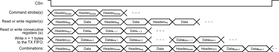 Figure 5-5 Register Access Types
5.6 Microcontroller Interface and Pin Configuration
In a typical system, CC115L will interface to a microcontroller. This microcontroller must be able to:
- Program CC115L into different modes
- Write buffered data
- Read back status information through the 4-wire SPI-bus configuration interface (SI, SO, SCLK, and CSn)
5.6.1 Configuration Interface
The microcontroller uses four I/O pins for the SPI configuration interface (SI, SO, SCLK, and CSn). The SPI is described in Section 5.5.
5.6.2 General Control and Status Pins
The CC115L has two dedicated configurable pins (GDO0 and GDO2) and one shared pin (GDO1) that can output internal status information useful for control software. These pins can be used to generate interrupts on the MCU. See Section 5.16 for more details on the signals that can be programmed.
GDO1 is shared with the SO pin in the SPI interface. The default setting for GDO1/SO is 3-state output. By selecting any other of the programming options, the GDO1/SO pin will become a generic pin. When CSn is low, the pin will always function as a normal SO pin.
In the synchronous and asynchronous serial modes, the GDO0 pin is used as a serial TX data input pin while in transmit mode.
5.7 Data Rate Programming
The data rate used when transmitting is programmed by the MDMCFG3.DRATE_M and the MDMCFG4.DRATE_E configuration registers. The data rate is given by the formula below. As the formula shows, the programmed data rate depends on the crystal frequency.
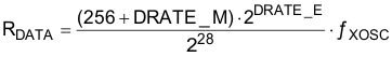
The following approach can be used to find suitable values for a given data rate:


If DRATE_M is rounded to the nearest integer and becomes 256, increment DRATE_E and use DRATE_M = 0.
The data rate can be set from 0.6 kBaud to 500 kBaud with the minimum step size according to Table 5-3. See Section 4.4 for the minimum and maximum data rates for the different modulation formats.
Table 5-3 Data Rate Step Size (Assuming a 26-MHz Crystal)
| Min Data Rate [kBaud] | Typical Data Rate [kBaud] | Max Data Rate [kBaud] | Data rate Step Size [kBaud] |
|---|---|---|---|
| 0.6 | 1.0 | 0.79 | 0.0015 |
| 0.79 | 1.2 | 1.58 | 0.0031 |
| 1.59 | 2.4 | 3.17 | 0.0062 |
| 3.17 | 4.8 | 6.33 | 0.0124 |
| 6.35 | 9.6 | 12.7 | 0.0248 |
| 12.7 | 19.6 | 25.3 | 0.0496 |
| 25.4 | 38.4 | 50.7 | 0.0992 |
| 50.8 | 76.8 | 101.4 | 0.1984 |
| 101.6 | 153.6 | 202.8 | 0.3967 |
| 203.1 | 250 | 405.5 | 0.7935 |
| 406.3 | 500 | 500 | 1.5869 |
5.8 Packet Handling Hardware Support
The CC115L has built-in hardware support for packet oriented radio protocols. The packet handler can be configured to add the following elements to the packet stored in the TX FIFO:
- A programmable number of preamble bytes
- A two byte synchronization (sync) word. Can be duplicated to give a 4-byte sync word. It is not possible to only insert preamble or only insert a sync word
- A CRC checksum computed over the data field.
- In a system where the CC115L is transmitting packets to the CC110L, CC113L or CC1101, the recommended setting is 4- byte preamble and 4-byte sync word, except for 500 kBaud data rate where the recommended preamble length is 8 bytes.
NOTE
Register fields that control the packet handling features should only be altered when CC115L is in the IDLE state.
5.8.1 Packet Format
The format of the data packet can be configured and consists of the following items (see Figure 5-6):
- Preamble
- Synchronization word
- Optional length byte
- Optional address byte
- Payload
- Optional 2 byte CRC
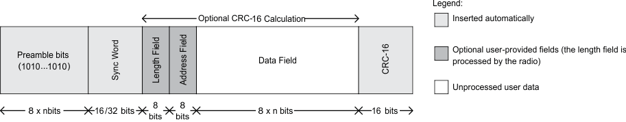 Figure 5-6 Packet Format
The preamble pattern is an alternating sequence of ones and zeros (10101010…). The minimum length of the preamble is programmable through the value of MDMCFG1.NUM_PREAMBLE. When enabling TX, the modulator will start transmitting the preamble. When the programmed number of preamble bytes has been transmitted, the modulator will send the sync word and then data from the TX FIFO if data is available. If the TX FIFO is empty, the modulator will continue to send preamble bytes until the first byte is written to the TX FIFO. The modulator will then send the sync word and then the data bytes.
The synchronization word is a two-byte value set in the SYNC1 and SYNC0 registers. If the CC110L, CC113L, or CC1101 are used at the receiving end, they will need the sync word for byte synchronization of the incoming packet. The synchronization word is automatically inserted by the CC115L. A one-byte sync word can be emulated by setting the SYNC1 value to the preamble pattern. It is also possible to emulate a 32 bit sync word by setting MDMCFG2.SYNC_MODE to 3. The sync word will then be repeated twice.
CC115L supports both constant packet length protocols and variable length protocols. Variable or fixed packet length mode can be used for packets up to 255 bytes. For longer packets, infinite packet length mode must be used.
Fixed packet length mode is selected by setting PKTCTRL0.LENGTH_CONFIG=0. The desired packet length is set by the PKTLEN register. This value must be different from 0.
In variable packet length mode, PKTCTRL0.LENGTH_CONFIG=1, the packet length is configured by the first byte transmitted after the sync word. The packet length is defined as the payload data, excluding the length byte and the optional CRC. The PKTLEN value must be different from 0.
With PKTCTRL0.LENGTH_CONFIG=2, the packet length is set to infinite and transmission will continue until turned off manually. As described in , this can be used to support packet formats with different length configuration than natively supported by CC115L. One should make sure that TX mode is not turned off during the transmission of the first half of any byte. Refer to the CC115L Errata Notes SWRZ036 for more details.
NOTE
The minimum packet length supported (excluding the optional length byte and CRC) is one byte of payload data.
5.8.1.1 Packet Length > 255
The packet automation control register, PKTCTRL0, can be reprogrammed during TX. This opens the possibility to transmit packets that are longer than 256 bytes and still be able to use the packet handling hardware support. At the start of the packet, the infinite packet length mode (PKTCTRL0.LENGTH_CONFIG=2) must be active and the PKTLEN register is set to mod(length, 256). When less than 256 bytes remains of the packet, the MCU disables infinite packet length mode and activates fixed packet length mode (PKTCTRL0.LENGTH_CONFIG=0). When the internal byte counter reaches the PKTLEN value, the transmission ends (the radio enters the state determined by TXOFF_MODE). Automatic CRC appending/checking can also be used (by setting PKTCTRL0.CRC_EN=1).
When for example a 600-byte packet is to be transmitted, the MCU should do the following (see Figure 5-7).
- Set PKTCTRL0.LENGTH_CONFIG=2.
- Pre-program the PKTLEN register to mod(600, 256) = 88.
- Transmit at least 345 bytes (600 - 255), for example by filling the 64-byte TX FIFO six times (384 bytes transmitted).
- Set PKTCTRL0.LENGTH_CONFIG=0.
- The transmission ends when the packet counter reaches 88. A total of 600 bytes are transmitted.
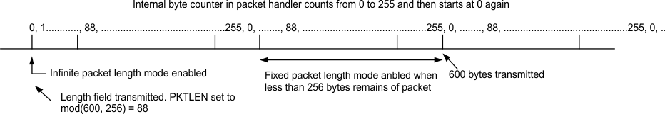 Figure 5-7 Packet Length > 255
5.8.2 Packet Handling
The payload that is to be transmitted must be written into the TX FIFO. The first byte written must be the length byte when variable packet length is enabled. The length byte has a value equal to the payload of the packet (including the optional address byte). If the receiver is the CC110L, CC113L, or CC1101, and address recognition is enabled, the second byte written to the TX FIFO must be the address byte.
If fixed packet length is enabled, the first byte written to the TX FIFO should be the address (assuming the receiver uses address recognition).
The modulator will first send the programmed number of preamble bytes. If data is available in the TX FIFO, the modulator will send the two-byte (optionally 4-byte) sync word followed by the payload in the TX FIFO. If CRC is enabled, the checksum is calculated over all the data pulled from the TX FIFO, and the result is sent as two extra bytes following the payload data. If the TX FIFO runs empty before the complete packet has been transmitted, the radio will enter TXFIFO_UNDERFLOW state. The only way to exit this state is by issuing an SFTX strobe. Writing to the TX FIFO after it has underflowed will not restart TX mode.
5.8.3 Packet Handling in Firmware
When implementing a packet oriented radio protocol in firmware, the MCU needs to know when a packet has been transmitted. Additionally, for packets longer than 64 bytes, the TX FIFO needs to be refilled while in TX. This means that the MCU needs to know the number of bytes that can be written to the TX FIFO. There are two possible solutions to get the necessary status information:
a. Interrupt Driven Solution
The GDO pins can be used to give an interrupt when a sync word has been transmitted or when a complete packet has been transmitted by setting IOCFGx.GDOx_CFG=0x06. In addition, there are two configurations for the IOCFGx.GDOx_CFG register that can be used as an interrupt source to provide information on how many bytes that are in the TX FIFO (IOCFGx.GDOx_CFG=0x02 and IOCFGx.GDOx_CFG=0x03). See Table 5-12 for more information.
b. SPI Polling
The PKTSTATUS register can be polled at a given rate to get information about the current GDO2 and GDO0 values respectively. The TXBYTES registers can be polled at a given rate to get information about the number of bytes in the and TX FIFO. Alternatively, the number of bytes in the TX FIFO can be read from the chip status byte returned on the MISO line each time a header byte, data byte, or command strobe is sent on the SPI bus.
It is recommended to employ an interrupt driven solution due to a small, but finite, probability that a single read from registers PKTSTATUS and TXBYTES is being corrupt. The same is the case when reading the chip status byte (see Section 5.5.3 and the CC115L Errata Notes SWRZ036).
5.9 Modulation Formats
CC115L supports amplitude, frequency, and phase shift modulation formats. The desired modulation format is set in the MDMCFG2.MOD_FORMAT register.
Optionally, the data stream can be Manchester coded by the modulator by setting MDMCFG2.MANCHESTER_EN=1.
NOTE
Manchester encoding is not supported at the same time as using 4-FSK modulation.
5.9.1 Frequency Shift Keying
CC115L supports 2-(G)FSK and 4-FSK modulation. When selecting 4-FSK, the preamble and sync word is sent using 2-FSK (see Figure 5-8).
The frequency deviation is programmed with the DEVIATION_M and DEVIATION_E values in the DEVIATN register. The value has an exponent/mantissa form, and the resultant deviation is given by:

The symbol encoding is shown in Table 5-4.
Table 5-4 Symbol Encoding for 2-FSK/GFSK and 4-FSK Modulation
| Format | Symbol | Coding |
|---|---|---|
| 2-FSK/GFSK | 0 | – Deviation |
| 1 | + Deviation | |
| 4-FSK | 01 | – Deviation |
| 00 | – 1/3×Deviation | |
| 10 | + 1/3×Deviation | |
| 11 | + Deviation |
 Figure 5-8 Data Sent Over the Air (MDMCFG2.MOD_FORMAT=100)
5.9.2 Amplitude Modulation
The amplitude modulation supported by CC115L is On-Off Keying (OOK). OOK modulation simply turns the PA on or off to modulate ones and zeros respectively.
The DEVIATN register setting has no effect when using OOK.
5.10 Radio Control
 Figure 5-9 Complete Radio Control State Diagram
CC115L has a built-in state machine that is used to switch between different operational states (modes). The change of state is done either by using command strobes or by internal events such as TX FIFO underflow.
A simplified state diagram, together with typical usage and current consumption, is shown in Figure 5-2. The complete radio control state diagram is shown in Figure 5-9. The numbers refer to the state number readable in the MARCSTATE status register. This register is primarily for test purposes.
5.10.1 Power-On Start-Up Sequence
When the power supply is turned on, the system must be reset. This is achieved by one of the two sequences described below, that is, automatic power-on reset (POR) or manual reset. After the automatic power-on reset or manual reset, it is also recommended to change the signal that is output on the GDO0 pin. The default setting is to output a clock signal with a frequency of CLK_XOSC/192. However, to optimize performance in TX, an alternative GDO setting from the settings found in Table 5-12 should be selected.
5.10.1.1 Automatic POR
A power-on reset circuit is included in the CC115L. The minimum requirements stated in Section 4.10 must be followed for the power-on reset to function properly. The internal power-up sequence is completed when CHIP_RDYn goes low. CHIP_RDYn is observed on the SO pin after CSn is pulled low. See Section 5.5.1 for more details on CHIP_RDYn.
When the CC115L reset is completed, the chip will be in the IDLE state and the crystal oscillator will be running. If the chip has had sufficient time for the crystal oscillator to stabilize after the power-on-reset, the SO pin will go low immediately after taking CSn low. If CSn is taken low before reset is completed, the SO pin will first go high, indicating that the crystal oscillator is not stabilized, before going low as shown in Figure 5-10.
 Figure 5-10 Power-On Reset with SRES
5.10.1.2 Manual Reset
The other global reset possibility on CC115L uses the SRES command strobe. By issuing this strobe, all internal registers and states are set to the default, IDLE state. The manual power-up sequence is as follows (see Figure 5-11):
- Set SCLK = 1 and SI = 0.
- Strobe CSn low / high.
- Hold CSn low and then high for at least 40 µs relative to pulling CSn low
- Pull CSn low and wait for SO to go low (CHIP_RDYn).
- Issue the SRES strobe on the SI line.
- When SO goes low again, reset is complete and the chip is in the IDLE state.
XOSC and voltage regulator switched on
 Figure 5-11 Power-On Reset with SRES
NOTE
The above reset procedure is only required just after the power supply is first turned on. If the user wants to reset the CC115L after this, it is only necessary to issue an SRES command strobe.
5.10.2 Crystal Control
The crystal oscillator (XOSC) is either automatically controlled or always on, if MCSM0.XOSC_FORCE_ON is set.
In the automatic mode, the XOSC will be turned off if the SXOFF or SPWD command strobes are issued; the state machine then goes to XOFF or SLEEP respectively. This can only be done from the IDLE state. The XOSC will be turned off when CSn is released (goes high). The XOSC will be automatically turned on again when CSn goes low. The state machine will then go to the IDLE state. The SO pin on the SPI interface must be pulled low before the SPI interface is ready to be used as described in Section 5.5.1.
If the XOSC is forced on, the crystal will always stay on even in the SLEEP state.
Crystal oscillator start-up time depends on crystal ESR and load capacitances. The electrical specification for the crystal oscillator can be found in Section 4.7.
5.10.3 Voltage Regulator Control
The voltage regulator to the digital core is controlled by the radio controller. When the chip enters the SLEEP state which is the state with the lowest current consumption, the voltage regulator is disabled. This occurs after CSn is released when a SPWD command strobe has been sent on the SPI interface. The chip is then in the SLEEP state. Setting CSn low again will turn on the regulator and crystal oscillator and make the chip enter the IDLE state.
5.10.4 Transmit Mode (TX)
Transmit mode is activated directly by the MCU by using the STX command strobe.
The frequency synthesizer must be calibrated regularly. CC115L has one manual calibration option (using the SCAL strobe), and three automatic calibration options that are controlled by the MCSM0.FS_AUTOCAL setting:
- Calibrate when going from IDLE to TX (or FSTXON)
- Calibrate when going from TX to IDLE automatically (not forced in IDLE by issuing an SIDLE strobe)
- Calibrate every fourth time when going from TX to IDLE automatically (not forced in IDLE by issuing an SIDLE strobe)
If the radio goes from TX to IDLE by issuing an SIDLE strobe, calibration will not be performed. The calibration takes a constant number of XOSC cycles; see Table 5-5 for timing details regarding calibration.
When TX is active the chip will remain in the TX state until the current packet has been successfully transmitted. Then the state will change as indicated by the MCSM1.TXOFF_MODE setting. The possible destinations are:
- IDLE
- FSTXON: Frequency synthesizer on and ready at the TX frequency. Activate TX with STX
- TX: Start sending preamble
The SIDLE command strobe can always be used to force the radio controller to go to the IDLE state.
5.10.5 Timing
5.10.5.1 Overall State Transition Times
The main radio controller needs to wait in certain states in order to make sure that the internal analog/digital parts have settled down and are ready to operate in the new states. A number of factors are important for the state transition times:
- The crystal oscillator frequency, fxosc
- OOK used or not
- The data rate in cases where OOK is used
- The value of the TEST0, TEST1, and FSCAL3 registers
Table 5-5 shows timing in crystal clock cycles for key state transitions.
Note that the TX to IDLE transition time is a function of data rate (fbaudrate). When OOK is used (that is, FREND0.PA_POWER=001b), TX to IDLE will require 1/8×f baudrate longer times than the time stated in Table 5-5.
Table 5-5 Overall State Transition Times [Example for 26-MHz Crystal Oscillator, 250 kBaud Data Rate, and TEST0 = 0x0B (Maximum Calibration Time)].
| Description | Transition Time (FREND0.PA_POWER=0) | Transition Time [µs] |
|---|---|---|
| IDLE to TX/FSTXON, no calibration | 1954/fxosc | 75.2 |
| IDLE to TX/FSTXON, with calibration | 1953/fxosc + FS calibration Time | 799 |
| TX to IDLE, no calibration | ~0.25/fbaudrate | ~1 |
| TX to IDLE, with calibration | ~0.25/fbaudrate + FS calibration Time | 725 |
| Manual calibration | 283/fxosc + FS calibration Time | 735 |
5.10.5.2 Frequency Synthesizer Calibration Time
Table 5-6 summarizes the frequency synthesizer (FS) calibration times for possible settings of TEST0 and FSCAL3.CHP_CURR_CAL_EN. Setting FSCAL3.CHP_CURR_CAL_EN to 00b disables the charge pump calibration stage. TEST0 is set to the values recommended by SmartRF Studio software SWRC176. The possible values for TEST0 when operating with different frequency bands are 0x09 and 0x0B. SmartRF Studio software always sets FSCAL3.CHP_CURR_CAL_EN to 10b.
The calibration time can be reduced from 712/724 µs to 145/157 µs. See Section 5.18.2 for more details.
Table 5-6 Frequency Synthesizer Calibration Times (26- and 27-MHz Crystal)
| TEST0 | FSCAL3.CHP_CURR_CAL_EN | FS Calibration Time fxosc = 26 MHz | FS Calibration Time fxosc = 27 MHz |
|---|---|---|---|
| 0x09 | 00b | 3764/fxosc = 145 µs | 3764/fxosc = 139 µs |
| 0x09 | 10b | 18506/fxosc = 712 µs | 18506/fxosc = 685 µs |
| 0x0B | 00b | 4073/fxosc = 157 µs | 4073/fxosc = 151 µs |
| 0x0B | 10b | 18815/fxosc = 724 µs | 18815/fxosc = 697 µs |
5.11 TX FIFO
The CC115L contains a 64-byte TX FIFO for data to be transmitted and the SPI interface is used to write to the TX FIFO (see Section 5.5.5 for more details). The FIFO controller will detect underflow in the TX FIFO.
When writing to the TX FIFO it is the responsibility of the MCU to avoid TX FIFO overflow. A TX FIFO overflow will result in an error in the TX FIFO content.
The chip status byte that is available on the SO pin while transferring the SPI header and contains the fill grade of the TX FIFO if the access is a write operation. Section 5.5.1 contains more details on this.
The number of bytes in the TX FIFO can be read from the status registers TXBYTES.NUM_TXBYTES.
The 4-bit FIFOTHR.FIFO_THR setting is used to program threshold points in the TX FIFO.
Table 5-7 lists the 16 FIFO_THR settings and the corresponding thresholds for the TX FIFO.
Table 5-7 FIFO_THR Settings and the Corresponding FIFO Thresholds
| FIFO_THR | Bytes in TX FIFO |
|---|---|
| 0 (0000) | 61 |
| 1 (0001) | 57 |
| 2 (0010) | 53 |
| 3 (0011) | 49 |
| 4 (0100) | 45 |
| 5 (0101) | 41 |
| 6 (0110) | 37 |
| 7 (0111) | 33 |
| 8 (1000) | 29 |
| 9 (1001) | 25 |
| 10 (1010) | 21 |
| 11 (1011) | 17 |
| 12 (1100) | 13 |
| 13 (1101) | 9 |
| 14 (1110) | 5 |
| 15 (1111) | 1 |
A signal will assert when the number of bytes in the TX FIFO is equal to or higher than the programmed threshold. This signal can be viewed on the GDO pins (see Table 5-12).
Figure 5-12 shows the number of bytes in the TX FIFO when the threshold signal toggles in the case of FIFO_THR=13. Figure 5-13 shows the signal on the GDO pin as the TX FIFO is filled above the threshold, and then drained below in the case of FIFO_THR=13.
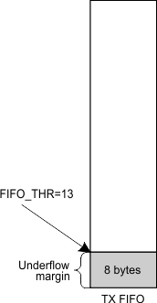 Figure 5-12 Example of FIFO at Threshold
 Figure 5-13 Number of Bytes in TX FIFO vs. the GDO Signal (GDOx_CFG=0x02 and FIFO_THR=13)
5.12 Frequency Programming
The frequency programming in CC115L is designed to minimize the programming needed when changing frequency.
To set up a system with channel numbers, the desired channel spacing is programmed with the MDMCFG0.CHANSPC_M and MDMCFG1.CHANSPC_E registers. The channel spacing registers are mantissa and exponent respectively. The base or start frequency is set by the 24 bit frequency word located in the FREQ2, FREQ1, and FREQ0 registers. This word will typically be set to the center of the lowest channel frequency that is to be used.
The desired channel number is programmed with the 8-bit channel number register, CHANNR.CHAN, which is multiplied by the channel offset. The resultant carrier frequency is given by:

With a 26 MHz crystal the maximum channel spacing is 405 kHz. To get that is, 1-MHz channel spacing, one solution is to use 333 kHz channel spacing and select each third channel in CHANNR.CHAN.
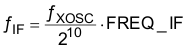
The preferred IF frequency is programmed with the FSCTRL1.FREQ_IF register. The IF frequency is given by:
If any frequency programming register is altered when the frequency synthesizer is running, the synthesizer may give an undesired response. Hence, the frequency should only be updated when the radio is in the IDLE state.
5.13 VCO
The VCO is completely integrated on-chip.
5.13.1 VCO and PLL Self-Calibration
The VCO characteristics vary with temperature and supply voltage changes as well as the desired operating frequency. In order to ensure reliable operation, CC115L includes frequency synthesizer self-calibration circuitry. This calibration should be done regularly, and must be performed after turning on power and before using a new frequency (or channel). The number of XOSC cycles for completing the PLL calibration is given in Table 5-5.
The calibration can be initiated automatically or manually. The synthesizer can be automatically calibrated each time the synthesizer is turned on, or each time the synthesizer is turned off automatically. This is configured with the MCSM0.FS_AUTOCAL register setting. In manual mode, the calibration is initiated when the SCAL command strobe is activated in the IDLE mode.
NOTE
The calibration values are maintained in SLEEP mode, so the calibration is still valid after waking up from SLEEP mode unless supply voltage or temperature has changed significantly.
To check that the PLL is in lock, the user can program register IOCFGx.GDOx_CFG to 0x0A, and use the lock detector output available on the GDOx pin as an interrupt for the MCU (x = 0, 1, or 2). A positive transition on the GDOx pin means that the PLL is in lock. As an alternative the user can read register FSCAL1. The PLL is in lock if the register content is different from 0x3F. Refer also to the CC115L Errata Notes SWRZ037.
For more robust operation, the source code could include a check so that the PLL is re-calibrated until PLL lock is achieved if the PLL does not lock the first time.
5.14 Voltage Regulators
CC115L contains several on-chip linear voltage regulators that generate the supply voltages needed by low-voltage modules. These voltage regulators are invisible to the user, and can be viewed as integral parts of the various modules. The user must however make sure that the absolute maximum ratings and required pin voltages in Table 3-1 and Table 5-1 are not exceeded.
By setting the CSn pin low, the voltage regulator to the digital core turns on and the crystal oscillator starts. The SO pin on the SPI interface must go low before the first positive edge of SCLK (setup time is given in Table 5-1).
If the chip is programmed to enter power-down mode (SPWD strobe issued), the power will be turned off after CSn goes high. The power and crystal oscillator will be turned on again when CSn goes low.
The voltage regulator for the digital core requires one external decoupling capacitor.
The voltage regulator output should only be used for driving the CC115L.
5.15 Output Power Programming
The RF output power level from the device has two levels of programmability. The PATABLE register can hold two user selected output power settings and the FREND0.PA_POWER value selects the PATABLE entry to use (0 or 1). PATABLE must be programmed in burst mode if writing to other entries than PATABLE[0]. See Section 5.5.6 for more programming details.
For OOK modulation, FREND0.PA_POWER should be 1 and the logic 0 and logic 1 power levels shall be programmed to index 0 and 1 respectively. For all other modulation formats, the desired output power should be programmed to index 0.
Table 5-8 contains the recommended PATABLE settings for various output levels and frequency bands. DN013 SWRA168 gives the complete tables for the different frequency bands using multi-layer inductors. Using PA settings from 0x61 to 0x6F is not allowed. Table 5-11 contains output power and current consumption for default PATABLE setting (0xC6). The measurements are done on SWRR045.
NOTE
All content of the PATABLE except for the first byte (index 0) is lost when entering the SLEEP state.
Table 5-8 Optimum PATABLE Settings for Various Output Power Levels Using Wire-Wound Inductors in 868- and 915-MHz Frequency Bands
| 868 MHz | 915 MHz | |||
|---|---|---|---|---|
| Output Power [dBm] | Setting | Current Consumption, Typ. [mA] | Setting | Current Consumption, Typ. [mA] |
| 12/11 | 0xC0 | 34.2 | 0xC0 | 33.4 |
| 10 | 0xC5 | 30.0 | 0xC3 | 30.7 |
| 7 | 0xCD | 25.8 | 0xCC | 25.7 |
| 5 | 0x86 | 19.9 | 0x84 | 20.2 |
| 0 | 0x50 | 16.8 | 0x8E | 17.2 |
| −6 | 0x37 | 16.4 | 0x38 | 17.0 |
| −10 | 0x26 | 14.5 | 0x27 | 14.8 |
| −15 | 0x1D | 13.3 | 0x1E | 13.3 |
| −20 | 0x17 | 12.6 | 0x0E | 12.5 |
| −30 | 0x03 | 12.0 | 0x03 | 11.9 |
Table 5-9 Output Power and Current Consumption for Default PATABLE Setting Using Wire-Wound Inductors in 868- and 915-MHz Frequency Bands
| 868 MHz | 915 MHz | |||
|---|---|---|---|---|
| Default Power Setting | Output Power [dBm] | Current Consumption, Typ. [mA] | Output Power [dBm] | Current Consumption, Typ. [mA] |
| 0xC6 | 9.6 | 29.4 | 8.9 | 28.7 |
Table 5-10 Optimum PATABLE Settings for Various Output Power Levels Using Multi-layer Inductors in 868- and 915-MHz Frequency Bands
| 868 MHz | 915 MHz | |||
|---|---|---|---|---|
| Output Power [dBm] | Setting | Current Consumption, Typ. [mA] | Setting | Current Consumption, Typ. [mA] |
| 10 | 0xC2 | 32.4 | 0xC0 | 31.8 |
| 7 | 0xCB | 26.8 | 0xC7 | 26.9 |
| 5 | 0x81 | 21.0 | 0xCD | 24.3 |
| 0 | 0x50 | 16.9 | 0x8E | 16.7 |
| −10 | 0x27 | 15.0 | 0x27 | 14.9 |
| −15 | 0x1E | 13.4 | 0x1E | 13.4 |
| −20 | 0x0F | 12.7 | 0x0E | 12.6 |
| −30 | 0x03 | 12.1 | 0x03 | 12.0 |
Table 5-11 Output Power and Current Consumption for Default PATABLE Setting Using Multi-layer Inductors in 868- and 915-MHz Frequency Bands
| 868 MHz | 915 MHz | |||
|---|---|---|---|---|
| Default Power Setting | Current Consumption, Typ. [mA] | Output Power [dBm] | Current Consumption, Typ. [mA] | Output Power [dBm] |
| 0xC6 | 8.5 | 29.5 | 7.2 | 27.4 |
5.16 General Purpose and Test Output Control Pins
The three digital output pins GDO0, GDO1, and GDO2 are general control pins configured with IOCFG0.GDO0_CFG, IOCFG1.GDO1_CFG, and IOCFG2.GDO2_CFG respectively. Table 5-12 shows the different signals that can be monitored on the GDO pins. These signals can be used as inputs to the MCU.
GDO1 is the same pin as the SO pin on the SPI interface, thus the output programmed on this pin will only be valid when CSn is high. The default value for GDO1 is 3-stated which is useful when the SPI interface is shared with other devices.
The default value for GDO0 is a 135–141 kHz clock output (XOSC frequency divided by 192). Since the XOSC is turned on at power-on-reset, this can be used to clock the MCU in systems with only one crystal. When the MCU is up and running, it can change the clock frequency by writing to IOCFG0.GDO0_CFG.
If the IOCFGx.GDOx_CFG setting is less than 0x20 and IOCFGx_GDOx_INV is 0 (1), the GDO0 and GDO2 pins will be hardwired to 0 (1), and the GDO1 pin will be hardwired to 1 (0) in the SLEEP state. These signals will be hardwired until the CHIP_RDYn signal goes low.
If the IOCFGx.GDOx_CFG setting is 0x20 or higher, the GDO pins will work as programmed also in SLEEP state. As an example, GDO1 is high impedance in all states if IOCFG1.GDO1_CFG=0x2E.
Table 5-12 GDOx Signal Selection (x = 0, 1, or 2)
| GDOx_CFG[5:0] | Description | |
|---|---|---|
| 0 (0x00) – 1 (0x01) | Reserved – used for test. | |
| 2 (0x02) | Associated to the TX FIFO: Asserts when the TX FIFO is filled at or above the TX FIFO threshold. Deasserts when the TX FIFO is below the same threshold. | |
| 3 (0x03) | Associated to the TX FIFO: Asserts when TX FIFO is full. Deasserts when the TX FIFO is drained below the TX FIFO threshold. | |
| 4 (0x04) | Reserved – used for test. | |
| 5 (0x05) | Asserts when the TX FIFO has underflowed. Deasserts when the FIFO is flushed. | |
| 6 (0x06) | Asserts when sync word has been sent, and de-asserts at the end of the packet. The pin will de-assert if the TX FIFO underflows. | |
| 7 (0x07) – 9 (0x09) | Reserved - used for test. | |
| 10 (0x0A) | Lock detector output. The PLL is in lock if the lock detector output has a positive transition or is constantly logic high. To check for PLL lock the lock detector output should be used as an interrupt for the MCU. | |
| 11 (0x0B) | Serial Clock. Synchronous to the data in synchronous serial mode. Data is sampled by CC 115L115L115L on the rising edge of the serial clock when GDOx_INV=0. | |
| 12 (0x0C) | Serial Synchronous Data Output. Used for synchronous serial mode. | |
| 13 (0x0D) | Serial Data Output. Used for asynchronous serial mode. | |
| 14 (0x0E) – 26 (0x1A) | Reserved - used for test. | |
| 27 (0x1B) | PA_PD. Note: PA_PD will have the same signal level in SLEEP and TX states. To control an external PA in applications where the SLEEP state is used it is recommended to use GDOx_CFGx=0x2F instead. | |
| 28 (0x1D) – 40 (0x28) | Reserved - used for test. | |
| 41 (0x29) | CHIP_RDYn | |
| 42 (0x2A) | Reserved - used for test. | |
| 43 (0x2B) | XOSC_STABLE | |
| 44 (0x2C) - 45 (0x2D) | Reserved - used for test. | |
| 46 (0x2E) | High impedance (3-state) | |
| 47 (0x2F) | HW to 0 (HW1 achieved by setting GDOx_INV=1). Can be used to control an external PA. | |
| 48 (0x30) | CLK_XOSC/1 | Note: There are 3 GDO pins, but only one CLK_XOSC/n can be selected as an output at any time. If CLK_XOSC/n is to be monitored on one of the GDO pins, the other two GDO pins must be configured to values less than 0x30. The GDO0 default value is CLK_XOSC/192. To optimize RF performance, these signals should not be used while the radio is in TX mode. |
| 49 (0x31) | CLK_XOSC/1.5 | |
| 50 (0x32) | CLK_XOSC/2 | |
| 51 (0x33) | CLK_XOSC/3 | |
| 52 (0x34) | CLK_XOSC/4 | |
| 53 (0x35) | CLK_XOSC/6 | |
| 54 (0x36) | CLK_XOSC/8 | |
| 55 (0x37) | CLK_XOSC/12 | |
| 56 (0x38) | CLK_XOSC/16 | |
| 57 (0x39) | CLK_XOSC/24 | |
| 58 (0x3A) | CLK_XOSC/32 | |
| 59 (0x3B) | CLK_XOSC/48 | |
| 60 (0x3C) | CLK_XOSC/64 | |
| 61 (0x3D) | CLK_XOSC/96 | |
| 62 (0x3E) | CLK_XOSC/128 | |
| 63 (0x3F) | CLK_XOSC/192 | |
5.17 Asynchronous and Synchronous Serial Operation
Several features and modes of operation have been included in the CC115L to provide backward compatibility with previous Chipcon products and other existing RF communication systems. For new systems, it is recommended to use the built-in packet handling features, as they can give more robust communication, significantly offload the microcontroller, and simplify software development.
5.17.1 Asynchronous Serial Operation
Asynchronous transfer is included in the CC115L for backward compatibility with systems that are already using the asynchronous data transfer.
When asynchronous transfer is enabled, all packet handling support is disabled and it is not possible to use Manchester encoding.
Asynchronous serial mode is enabled by setting PKTCTRL0.PKT_FORMAT to 3. Strobing STX will configure the GDO0 pin as data input (TX data) regardless of the content of the IOCFG0 register. Data output can be on GDO0, GDO1, or GDO2. This is set by the IOCFG0.GDO0_CFG, IOCFG1.GDO1_CFG and IOCFG2.GDO2_CFG fields.
The CC115L modulator samples the level of the asynchronous input 8 times faster than the programmed data rate. The timing requirement for the asynchronous stream is that the error in the bit period must be less than one eighth of the programmed data rate.
5.17.2 Synchronous Serial Operation
Setting PKTCTRL0.PKT_FORMAT to 1 enables synchronous serial mode. When using this mode, sync detection should be disabled together with CRC calculation (MDMCFG2.SYNC_MODE=000 and PKTCTRL0.CRC_EN=0). Infinite packet length mode should be used (PKTCTRL0.LENGTH_CONFIG=10b).
In synchronous serial mode, data is transferred on a two-wire serial interface. The CC115L provides a clock that is used to set up new data on the data input line or sample data on the data output line. Data input (TX data) is on the GDO0 pin. This pin will automatically be configured as an input when TX is active. The TX latency is 8 bits.
The MCU must handle preamble and sync word insertion/detection in software, together with CRC calculation and insertion.
5.18 System Considerations and Guidelines
5.18.1 SRD Regulations
International regulations and national laws regulate the use of radio receivers and transmitters. Short Range Devices (SRDs) for license free operation below 1 GHz are usually operated in the 315 MHz, 433 MHz, 868 MHz, or 915 MHz frequency bands. The CC115L is specifically designed for such use with its 300–348 MHz, 387–464 MHz, and 779–928 MHz operating ranges. The most important regulations when using the CC115L in the 315 MHz, 433 MHz, 868 MHz, or 915 MHz frequency bands are EN 300 220 V2.3.1 (Europe) and FCC CFR47 Part 15 (USA).
For compliance with modulation bandwidth requirements under EN 300 220 V2.3.1 in the 863 to 870 MHz frequency range it is recommended to use a 26-MHz crystal for frequencies below 869 MHz and a 27 MHz crystal for frequencies above 869 MHz.
Compliance with regulations is dependent on the complete system performance. It is the customer's responsibility to ensure that the system complies with regulations.
5.18.2 Calibration in Multi-Channel Systems
CC115L is highly suited for multi-channel systems due to its agile frequency synthesizer and effective communication interface.
Charge pump current, VCO current, and VCO capacitance array calibration data is required for each frequency when implementing a multi-channel system. There are 3 ways of obtaining the calibration data from the chip:
- Calibration for every frequency change. The PLL calibration time is 712/724 μs (26 MHz crystal and TEST0 = 0x09/0B, see Table 5-6). The blanking interval between each frequency hop is then 787/799 µs.
- Perform all necessary calibration at startup and store the resulting FSCAL3, FSCAL2, and FSCAL1 register values in MCU memory. The VCO capacitance calibration FSCAL1 register value must be found for each RF frequency to be used. The VCO current calibration value and the charge pump current calibration value available in FSCAL2 and FSCAL3 respectively are not dependent on the RF frequency, so the same value can therefore be used for all RF frequencies for these two registers. Between each frequency hop, the calibration process can then be replaced by writing the FSCAL3, FSCAL2 and FSCAL1 register values that corresponds to the next RF frequency. The PLL turn on time is approximately 75 µs (see Table 5-5). The blanking interval between each frequency hop is then approximately 75 µs.
- Run calibration on a single frequency at startup. Next write 0 to FSCAL3[5:4] to disable the charge pump calibration. After writing to FSCAL3[5:4], strobe STX with MCSM0.FS_AUTOCAL=1 for each new frequency hop. That is, VCO current and VCO capacitance calibration is done, but not charge pump current calibration. When charge pump current calibration is disabled the calibration time is reduced from 712/724 µs to 145/157 µs (26 MHz crystal and TEST0 = 0x09/0B, see Table 5-6). The blanking interval between each frequency hop is then 220/232 µs.
There is a trade off between blanking time and memory space needed for storing calibration data in non-volatile memory. Solution 2) above gives the shortest blanking interval, but requires more memory space to store calibration values. This solution also requires that the supply voltage and temperature do not vary much in order to have a robust solution. Solution 3) gives 567 µs smaller blanking interval than solution 1).
The recommended settings for TEST0.VCO_SEL_CAL_EN change with frequency. This means that one should always use SmartRF Studio to get the correct settings for a specific frequency before doing a calibration, regardless of which calibration method is being used.
NOTE
The content in the TEST0 register is not retained in SLEEP state, thus it is necessary to re-write this register when returning from the SLEEP state.
5.18.3 Wideband Modulation when not Using Spread Spectrum
Digital modulation systems under FCC Section 15.247 include 2-FSK, GFSK, and 4-FSK modulation. A maximum peak output power of 1 W (+30 dBm) is allowed if the 6 dB bandwidth of the modulated signal exceeds 500 kHz. In addition, the peak power spectral density conducted to the antenna shall not be greater than +8 dBm in any 3 kHz band.
Operating at high data rates and frequency separation, the CC115L is suited for systems targeting compliance with digital modulation system as defined by FCC Section 15.247. An external power amplifier such as CC1190 SWRS089 is needed to increase the output above +11 dBm. Refer to DN006 SWRA123 for further details concerning wideband modulation and CC115L.
5.18.4 Data Burst Transmissions
The high maximum data rate of CC115L opens up for burst transmissions. A low average data rate link (e.g. 10 kBaud) can be realized by using a higher over-the-air data rate. Buffering the data and transmitting in bursts at high data rate (e.g. 500 kBaud) will reduce the time in TX mode, and hence also reduce the average current consumption significantly. Reducing the time in TX mode will reduce the likelihood of collisions with other systems in the same frequency range.
5.18.5 Continuous Transmissions
In data streaming applications, the CC115L opens up for continuous transmissions at 500 kBaud effective data rate. As the modulation is done with a closed loop PLL, there is no limitation in the length of a transmission (open loop modulation used in some radios often prevents this kind of continuous data streaming and reduces the effective data rate).
5.18.6 Increasing Output Power
The PA portion of the CC1190 SWRS089 can be used together with CC115L in applications where increased output power is needed.
5.19 Configuration Registers
The configuration of CC115L is done by programming 8-bit registers. The optimum configuration data based on selected system parameters are most easily found by using the SmartRF Studio software SWRC176. Complete descriptions of the registers are given in the following tables. After chip reset, all the registers have default values as shown in the tables. The optimum register setting might differ from the default value. After a reset, all registers that shall be different from the default value therefore needs to be programmed through the SPI interface.
There are 9 command strobe registers, listed in Table 5-13. Accessing these registers will initiate the change of an internal state or mode. There are 34 normal 8-bit configuration registers listed in Table 5-14 and SmartRF Studio SWRC176 will provide recommended settings for these registers (Addresses marked as “Not Used” can be part of a burst access and one can write a dummy value to them. Addresses marked as “Reserved” must be configured according to SmartRF Studio SWRC176).
There are also 5 status registers that are listed in Table 5-15. These registers, which are read-only, contain information about the status of CC115L.
The TX FIFO is accessed through one 8-bit register. During the header byte transfer and while writing data to a register or the TX FIFO, a status byte is returned on the SO line. This status byte is described in Table 5-2.
Table 5-16 summarizes the SPI address space. The address to use is given by adding the base address to the left and the burst and read/write bits on the top. Note that the burst bit has different meaning for base addresses above and below 0x2F.
Table 5-13 Command Strobes
| Address | Strobe Name | Description |
|---|---|---|
| 0x30 | SRES | Reset chip. |
| 0x31 | SFSTXON | Enable and calibrate frequency synthesizer (if MCSM0.FS_AUTOCAL=1). |
| 0x32 | SXOFF | Turn off crystal oscillator. |
| 0x33 | SCAL | Calibrate frequency synthesizer and turn it off. SCAL can be strobed from IDLE mode without setting manual calibration mode (MCSM0.FS_AUTOCAL=0) |
| 0x34 | Reserved | |
| 0x35 | STX | In IDLE state: Enable TX. Perform calibration first if MCSM0.FS_AUTOCAL=1. |
| 0x36 | SIDLE | Enter IDLE state |
| 0x37 - 0x38 | Reserved | |
| 0x39 | SPWD | Enter power down mode when CSn goes high. |
| 0x3A | Reserved | |
| 0x3B | SFTX | Flush the TX FIFO buffer. Only issue SFTX in IDLE or TXFIFO_UNDERFLOW states. |
| 0x3C | Reserved | |
| 0x3D | SNOP | No operation. May be used to get access to the chip status byte. |
Table 5-14 Configuration Registers Overview
| Address | Register | Description | Preserved in SLEEP State | Details on Page Number |
|---|---|---|---|---|
| 0x00 | IOCFG2 | GDO2 output pin configuration | Yes | Table 5-17 |
| 0x01 | IOCFG1 | GDO1 output pin configuration | Yes | Table 5-18 |
| 0x02 | IOCFG0 | GDO0 output pin configuration | Yes | Table 5-19 |
| 0x03 | FIFOTHR | TX FIFO thresholds | Yes | Table 5-20 |
| 0x04 | SYNC1 | Sync word, high byte | Yes | Table 5-21 |
| 0x05 | SYNC0 | Sync word, low byte | Yes | Table 5-22 |
| 0x06 | PKTLEN | Packet length | Yes | Table 5-23 |
| 0x07 | Not used | |||
| 0x08 | PKTCTRL0 | Packet automation control | Yes | Table 5-24 |
| 0x09 | Not used | |||
| 0x0A | CHANNR | Channel number | Yes | Table 5-25 |
| 0x0B | Not used | |||
| 0x0C | FSCTRL0 | Frequency synthesizer control | Yes | Table 5-26 |
| 0x0D | FREQ2 | Frequency control word, high byte | Yes | Table 5-27 |
| 0x0E | FREQ1 | Frequency control word, middle byte | Yes | Table 5-28 |
| 0x0F | FREQ0 | Frequency control word, low byte | Yes | Table 5-29 |
| 0x10 | MDMCFG4 | Modem configuration | Yes | Table 5-30 |
| 0x11 | MDMCFG3 | Modem configuration | Yes | Table 5-31 |
| 0x12 | MDMCFG2 | Modem configuration | Yes | Table 5-32 |
| 0x13 | MDMCFG1 | Modem configuration | Yes | Table 5-33 |
| 0x14 | MDMCFG0 | Modem configuration | Yes | Table 5-34 |
| 0x15 | DEVIATN | Modem deviation setting | Yes | Table 5-35 |
| 0x16 | Not used | |||
| 0x17 | MCSM1 | Main Radio Control State Machine configuration | Yes | Table 5-36 |
| 0x18 | MCSM0 | Main Radio Control State Machine configuration | Yes | Table 5-37 |
| 0x19 - 0x1F | Not Used | |||
| 0x20 | RESERVED | Yes | Table 5-38 | |
| 0x21 | Not Used | |||
| 0x22 | FREND0 | Front end TX configuration | Yes | Table 5-39 |
| 0x23 | FSCAL3 | Frequency synthesizer calibration | Yes | Table 5-40 |
| 0x24 | FSCAL2 | Frequency synthesizer calibration | Yes | Table 5-41 |
| 0x25 | FSCAL1 | Frequency synthesizer calibration | Yes | Table 5-42 |
| 0x26 | FSCAL0 | Frequency synthesizer calibration | Yes | Table 5-43 |
| 0x27 - 0x28 | Not Used | |||
| 0x29 - 0x2B | RESERVED | No | Table 5-44 | |
| 0x2C | TEST2 | Various test settings | No | Table 5-47 |
| 0x2D | TEST1 | Various test settings | No | Table 5-48 |
| 0x2E | TEST0 | Various test settings | No | Table 5-49 |
Table 5-15 Status Registers Overview
| Address | Register | Description | Details on page number |
|---|---|---|---|
| 0x30 (0xF0) | PARTNUM | Part number for CC115L | Table 5-50 |
| 0x31 (0xF1) | VERSION | Current version number | Table 5-51 |
| 0x32 – 0x34 (0xF2 – 0xF4) | Reserved | ||
| 0x35 (0xF5) | MARCSTATE | Control state machine state | Table 5-52 |
| 0x36 - 0x37 (0xF6 – 0xF7) | Reserved | ||
| 0x38 (0xF8) | PKTSTATUS | Current GDOx status and packet status | Table 5-53 |
| 0x39 (0xF9) | Reserved | ||
| 0x3A (0xFA) | TXBYTES | Underflow and number of bytes in the TX FIFO | Table 5-54 |
| 0x3B - 0x3D (0xFB - 0xFD) | Reserved |
Table 5-16 SPI Address Space
| Write | Read | ||||
|---|---|---|---|---|---|
| Single Byte | Burst | Single Byte | Burst | ||
| +0x00 | +0x40 | +0x80 | +0xC0 | ||
| 0x00 | IOCFG2 | R/W configuration registers, burst access possible | |||
| 0x01 | IOCFG1 | ||||
| 0x02 | IOCFG0 | ||||
| 0x03 | FIFOTHR | ||||
| 0x04 | SYNC1 | ||||
| 0x05 | SYNC0 | ||||
| 0x06 | PKTLEN | ||||
| 0x07 | Not Used | ||||
| 0x08 | PKTCTRL0 | ||||
| 0x09 | Not Used | ||||
| 0x0A | CHANNR | ||||
| 0x0B | Not Used | ||||
| 0x0C | FSCTRL0 | ||||
| 0x0D | FREQ2 | ||||
| 0x0E | FREQ1 | ||||
| 0x0F | FREQ0 | ||||
| 0x10 | MDMCFG4 | ||||
| 0x11 | MDMCFG3 | ||||
| 0x12 | MDMCFG2 | ||||
| 0x13 | MDMCFG1 | ||||
| 0x14 | MDMCFG0 | ||||
| 0x15 | DEVIATN | ||||
| 0x16 | Not Used | ||||
| 0x17 | MCSM1 | ||||
| 0x18 | MCSM0 | ||||
| 0x19 | Not Used | ||||
| 0x1A | Not Used | ||||
| 0x1B | Not Used | ||||
| 0x1C | Not Used | ||||
| 0x1D | Not Used | ||||
| 0x1E | Not Used | ||||
| 0x1F | Not Used | ||||
| 0x20 | Not Used | ||||
| 0x21 | Not Used | ||||
| 0x22 | FREND0 | ||||
| 0x23 | FSCAL3 | ||||
| 0x24 | FSCAL2 | ||||
| 0x25 | FSCAL1 | ||||
| 0x26 | FSCAL0 | ||||
| 0x27 | Not Used | ||||
| 0x28 | Not Used | ||||
| 0x29 | RESERVED | ||||
| 0x2A | RESERVED | ||||
| 0x2B | RESERVED | ||||
| 0x2C | TEST2 | ||||
| 0x2D | TEST1 | ||||
| 0x2E | TEST0 | ||||
| 0x2F | Not Used | ||||
| 0x30 | SRES | SRES | PARTNUM | Command Strobes, Status registers (read only) and multi byte registers | |
| 0x31 | SFSTXON | SFSTXON | VERSION | ||
| 0x32 | SXOFF | SXOFF | Reserved | ||
| 0x33 | SCAL | SCAL | Reserved | ||
| 0x34 | Not Used | Reserved | Reserved | ||
| 0x35 | STX | STX | MARCSTATE | ||
| 0x36 | SIDLE | SIDLE | Reserved | ||
| 0x37 | Reserved | Reserved | Reserved | ||
| 0x38 | Reserved | Reserved | PKTSTATUS | ||
| 0x39 | SPWD | SPWD | Reserved | ||
| 0x3A | Reserved | Reserved | TXBYTES | ||
| 0x3B | SFTX | SFTX | Reserved | ||
| 0x3C | Reserved | Reserved | Reserved | ||
| 0x3D | SNOP | SNOP | Reserved | ||
| 0x3E | PATABLE | PATABLE | PATABLE | PATABLE | |
| 0x3F | TX FIFO | TX FIFO | Reserved | Reserved | |
5.19.1 Configuration Register Details - Registers with preserved values in SLEEP state
Table 5-17 0x00: IOCFG2 - GDO2 Output Pin Configuration
| Bit | Field Name | Reset | R/W | Description |
|---|---|---|---|---|
| 7 | R0 | Not used | ||
| 6 | GDO2_INV | 0 | R/W | Invert output, that is, select active low (1) / high (0) |
| 5:0 | GDO2_CFG[5:0] | 41 (101001) | R/W | Default is CHP_RDYn (see Table 5-12). |
Table 5-18 0x01: IOCFG1 - GDO1 Output Pin Configuration
| Bit | Field Name | Reset | R/W | Description |
|---|---|---|---|---|
| 7 | GDO_DS | 0 | R/W | Set high (1) or low (0) output drive strength on the GDO pins. |
| 6 | GDO1_INV | 0 | R/W | Invert output, that is, select active low (1) / high (0) |
| 5:0 | GDO1_CFG[5:0] | 46 (101110) | R/W | Default is 3-state (see Table 5-12). |
Table 5-19 0x02: IOCFG0 - GDO0 Output Pin Configuration
| Bit | Field Name | Reset | R/W | Description |
|---|---|---|---|---|
| 7 | 0 | R/W | Use setting from SmartRF Studio | |
| 6 | GDO0_INV | 0 | R/W | Invert output, that is, select active low (1) / high (0) |
| 5:0 | GDO0_CFG[5:0] | 63 (0x3F) | R/W | Default is CLK_XOSC/192 (see Table 5-12). It is recommended to disable the clock output in initialization, in order to optimize RF performance. |
Table 5-20 0x03: FIFOTHR - TX FIFO Thresholds
| Bit | Field Name | Reset | R/W | Description | ||
|---|---|---|---|---|---|---|
| 7:4 | 0 | R/W | Use setting from SmartRF Studio | |||
| 3:0 | FIFO_THR[3:0] | 7 (0111) | R/W | Set the threshold for the TX FIFO. The threshold is exceeded when the number of bytes in the TX FIFO is equal to or higher than the threshold value. | ||
| Setting | Bytes in TX FIFO | |||||
| 0 (0000) | 61 | |||||
| 1 (0001) | 57 | |||||
| 2 (0010) | 53 | |||||
| 3 (0011) | 49 | |||||
| 4 (0100) | 45 | |||||
| 5 (0101) | 41 | |||||
| 6 (0110) | 37 | |||||
| 7 (0111) | 33 | |||||
| 8 (1000) | 29 | |||||
| 9 (1001) | 25 | |||||
| 10 (1010) | 21 | |||||
| 11 (1011) | 17 | |||||
| 12 (1100) | 13 | |||||
| 13 (1101) | 9 | |||||
| 14 (1110) | 5 | |||||
| 15 (1111) | 1 | |||||
Table 5-21 0x04: SYNC1 - Sync Word, High Byte
| Bit | Field Name | Reset | R/W | Description |
|---|---|---|---|---|
| 7:0 | SYNC[15:8] | 211 (0xD3) | R/W | 8 MSB of 16-bit sync word |
Table 5-22 0x05: SYNC0 - Sync Word, Low Byte
| Bit | Field Name | Reset | R/W | Description |
|---|---|---|---|---|
| 7:0 | SYNC[7:0] | 145 (0x91) | R/W | 8 LSB of 16-bit sync word |
Table 5-23 0x06: PKTLEN - Packet Length
| Bit | Field Name | Reset | R/W | Description |
|---|---|---|---|---|
| 7:0 | PACKET_LENGTH | 255 (0xFF) | R/W | Indicates the packet length when fixed packet length mode is enabled. This value must be different from 0. |
Table 5-24 0x08: PKTCTRL0 - Packet Automation Control
| Bit | Field Name | Reset | R/W | Description | |
|---|---|---|---|---|---|
| 7 | R0 | Not used | |||
| 6 | 1 | R/W | Use setting from SmartRF Studio | ||
| 5:4 | PKT_FORMAT[1:0] | 0 (00) | R/W | Format of TX data | |
| Setting | Packet format | ||||
| 0 (00) | Normal mode, use TX FIFO | ||||
| 1 (01) | Synchronous serial mode, Data in on GDO0 | ||||
| 2 (10) | Random TX mode; sends random data using PN9 generator. Used for test. | ||||
| 3 (11) | Asynchronous serial mode, Data in on GDO0 | ||||
| 3 | 0 | R0 | Not used | ||
| 2 | CRC_EN | 1 | R/W | 1: CRC calculation enabled | |
| 0: CRC calculation disabled | |||||
| 1:0 | LENGTH_CONFIG[1:0] | 1 (01) | R/W | Configure the packet length | |
| Setting | Packet length configuration | ||||
| 0 (00) | Fixed packet length mode. Length configured in PKTLEN register | ||||
| 1 (01) | Variable packet length mode. Packet length configured by the first byte written to the TX FIFO | ||||
| 2 (10) | Infinite packet length mode | ||||
| 3 (11) | Reserved | ||||
Table 5-25 0x0A: CHANNR - Channel Number
| Bit | Field Name | Reset | R/W | Description |
|---|---|---|---|---|
| 7:0 | CHAN[7:0] | 0 (0x00) | R/W | The 8-bit unsigned channel number, which is multiplied by the channel spacing setting and added to the base frequency. |
Table 5-26 0x0C: FSCTRL0 - Frequency Synthesizer Control
| Bit | Field Name | Reset | R/W | Description |
|---|---|---|---|---|
| 7:0 | FREQOFF[7:0] | 0 (0x00) | R/W | Frequency offset added to the base frequency before being used by the frequency synthesizer. (2s-complement). Resolution is FXTAL/214 (1.59kHz-1.65kHz); range is ±202 kHz to ±210 kHz, dependent of XTAL frequency. |
Table 5-27 0x0D: FREQ2 - Frequency Control Word, High Byte
| Bit | Field Name | Reset | R/W | Description |
|---|---|---|---|---|
| 7:6 | FREQ[23:22] | 0 (00) | R | FREQ[23:22] is always 0 (the FREQ2 register is less than 36 with 26 - 27 MHz crystal) |
| 5:0 | FREQ[21:16] | 30 (011110) | R/W | FREQ[23:0] is the base frequency for the frequency synthesizer in increments of fXOSC/216.  |
Table 5-28 0x0E: FREQ1 - Frequency Control Word, Middle Byte
| Bit | Field Name | Reset | R/W | Description |
|---|---|---|---|---|
| 7:0 | FREQ[15:8] | 196 (0xC4) | R/W | See Table 5-27. |
Table 5-29 0x0F: FREQ0 - Frequency Control Word, Low Byte
| Bit | Field Name | Reset | R/W | Description |
|---|---|---|---|---|
| 7:0 | FREQ[7:0] | 236 (0xEC) | R/W | See Table 5-27. |
Table 5-30 0x10: MDMCFG4 - Modem Configuration
| Bit | Field Name | Reset | R/W | Description |
|---|---|---|---|---|
| 7:4 | 8 (1000) | R/W | Use setting from SmartRF Studio SWRC176 | |
| 3:0 | DRATE_E[3:0] | 12 (1100) | R/W | The exponent of the user specified symbol rate |
Table 5-31 0x11: MDMCFG3 - Modem Configuration
| Bit | Field Name | Reset | R/W | Description |
|---|---|---|---|---|
| 7:0 | DRATE_M[7:0] | 34 (0x22) | R/W | The mantissa of the user specified symbol rate. The symbol rate is configured using an unsigned, floating-point number with 9-bit mantissa and 4-bit exponent. The 9th bit is a hidden '1'. The resulting data rate is:  |
Table 5-32 0x12: MDMCFG2 - Modem Configuration
| Bit | Field Name | Reset | R/W | Description | |
|---|---|---|---|---|---|
| 7 | 0 | R/W | Use setting from SmartRF Studio SWRC176 | ||
| 6:4 | MOD_FORMAT[2:0] | 0 (000) | R/W | The modulation format of the radio signal | |
| Setting | Modulation format | ||||
| 0 (000) | 2-FSK | ||||
| 1 (001) | GFSK | ||||
| 2 (010) | Reserved | ||||
| 3 (011) | OOK | ||||
| 4 (100) | 4-FSK | ||||
| 5 (101) | Reserved | ||||
| 6 (110) | Reserved | ||||
| 7 (111) | Reserved | ||||
| 4-FSK modulation cannot be used together with Manchester encoding | |||||
| 3 | MANCHESTER_EN | 0 | R/W | Enables Manchester encoding/decoding. | |
| 0 = Disable | |||||
| 1 = Enable | |||||
| Manchester encoding cannot be used when using asynchronous serial mode or 4-FSK modulation | |||||
| 2:0 | SYNC_MODE[2:0] | 2 (010) | R/W | Number of sync bits transmitted | |
| Setting | Sync-word qualifier mode | ||||
| 0 (000) | No preamble/sync | ||||
| 1 (001) | 16-bits sync word | ||||
| 2 (010) | Reserved | ||||
| 3 (011) | 32-bits sync word | ||||
| 4 (100) – 7 (111) | Reserved | ||||
Table 5-33 0x13: MDMCFG1 - Modem Configuration
| Bit | Field Name | Reset | R/W | Description | |
|---|---|---|---|---|---|
| 7 | 0 | R/W | Use setting from SmartRF Studio SWRC176 | ||
| 6:4 | NUM_PREAMBLE[2:0] | 2 (010) | R/W | Sets the minimum number of preamble bytes to be transmitted | |
| Setting | Number of preamble bytes | ||||
| 0 (000) | 2 | ||||
| 1 (001) | 3 | ||||
| 2 (010) | 4 | ||||
| 3 (011) | 6 | ||||
| 4 (100) | 8 | ||||
| 5 (101) | 12 | ||||
| 6 (110) | 16 | ||||
| 7 (111) | 24 | ||||
| 3:2 | R0 | Not used | |||
| 1:0 | CHANSPC_E[1:0] | 2 (10) | R/W | 2 bit exponent of channel spacing | |
Table 5-34 0x14: MDMCFG0 - Modem Configuration
| Bit | Field Name | Reset | R/W | Description |
|---|---|---|---|---|
| 7:0 | CHANSPC_M[7:0] | 248 (0xF8) | R/W | 8-bit mantissa of channel spacing. The channel spacing is multiplied by the channel number CHAN and added to the base frequency. It is unsigned and has the format: 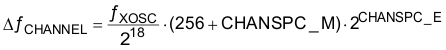 |
Table 5-35 0x15: DEVIATN - Modem Deviation Setting
| Bit | Field Name | Reset | R/W | Description | |
|---|---|---|---|---|---|
| 7 | R0 | Not used. | |||
| 6:4 | DEVIATION_E[2:0] | 4 (100) | R/W | Deviation exponent. | |
| 3 | R0 | Not used. | |||
| 2:0 | DEVIATION_M[2:0] | 7 (111) | R/W | 2-FSK/GFSK/4-FSK | Specifies the nominal frequency deviation from the carrier for a '0' (-DEVIATN) and '1' (+DEVIATN) in a mantissa- exponent format, interpreted as a 4-bit value with MSB implicit 1. The resulting frequency deviation is given by: 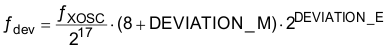 |
| OOK | This setting has no effect | ||||
Table 5-36 0x17: MCSM1 - Main Radio Control State Machine Configuration
| Bit | Field Name | Reset | R/W | Description | |
|---|---|---|---|---|---|
| 7:6 | R0 | Not used | |||
| 5:2 | 3 (1100) | R/W | Use setting from SmartRF Studio SWRC176 | ||
| 1:0 | TXOFF_MODE[1:0] | 0 (00) | R/W | Select what should happen when a packet has been sent | |
| Setting | Next state after finishing packet transmission | ||||
| 0 (00) | IDLE | ||||
| 1 (01) | FSTXON | ||||
| 2 (10) | Stay in TX (start sending preamble) | ||||
| 3 (11) | Reserved | ||||
Table 5-37 0x18: MCSM0 - Main Radio Control State Machine Configuration
| Bit | Field Name | Reset | R/W | Description | ||
|---|---|---|---|---|---|---|
| 7:6 | R0 | Not used | ||||
| 5:4 | FS_AUTOCAL[1:0] | 0 (00) | R/W | Automatically calibrate when going to or from TX mode | ||
| Setting | When to perform automatic calibration | |||||
| 0 (00) | Never (manually calibrate using SCAL strobe) | |||||
| 1 (01) | When going from IDLE to TX (or FSTXON) | |||||
| 2 (10) | When going from TX back to IDLE automatically | |||||
| 3 (11) | Every 4th time when going from TX to IDLE automatically | |||||
| 3:2 | PO_TIMEOUT | 1 (01) | R/W | Programs the number of times the six-bit ripple counter must expire after the XOSC has settled before CHP_RDYn goes low.(1)
If XOSC is on (stable) during power-down, PO_TIMEOUT shall be set so that the regulated digital supply voltage has time to stabilize before CHP_RDYn goes low (PO_TIMEOUT=2 recommended). Typical start-up time for the voltage regulator is 50 μs. For robust operation it is recommended to use PO_TIMEOUT = 2 or 3 when XOSC is off during power-down. |
||
| Setting | Expire count | Timeout after XOSC start | ||||
| 0 (00) | 1 | Approximately 2.3 - 2.4 μs | ||||
| 1 (01) | 16 | Approximately 37 - 39 μs | ||||
| 2 (10) | 64 | Approximately 149 - 155 μs | ||||
| 3 (11) | 256 | Approximately 597 - 620 μs | ||||
| Exact timeout depends on crystal frequency. | ||||||
| 1 | 0 | R/W | Use setting from SmartRF Studio SWRC176 | |||
| 0 | XOSC_FORCE_ON | 0 | R/W | Force the XOSC to stay on in the SLEEP state. | ||
Table 5-38 0x20: RESERVED
| Bit | Field Name | Reset | R/W | Description |
|---|---|---|---|---|
| 7:3 | 31 (11111) | R/W | Use setting from SmartRF Studio SWRC176 | |
| 2 | R0 | Not used | ||
| 1:0 | 0 (00) | R/W | Use setting from SmartRF Studio SWRC176 |
Table 5-39 0x22: FREND0 - Front End TX Configuration
| Bit | Field Name | Reset | R/W | Description |
|---|---|---|---|---|
| 7:6 | R0 | Not used | ||
| 5:4 | LODIV_BUF_CURRENT_TX[1:0] | 1 (01) | R/W | Adjusts current TX LO buffer (input to PA). The value to use in this field is given by the SmartRF Studio software SWRC176. |
| 3 | R0 | Not used | ||
| 2:0 | PA_POWER[2:0] | 0 (000) | R/W | Selects PA power setting. This value is an index to the PATABLE, which can be programmed with up to 2 different PA settings. When using OOK, PA_POWER should be 001, and for all other modulation formats it should be 000, see Section 5.5.6. |
Table 5-40 0x23: FSCAL3 - Frequency Synthesizer Calibration
| Bit | Field Name | Reset | R/W | Description |
|---|---|---|---|---|
| 7:6 | FSCAL3[7:6] | 2 (10) | R/W | Frequency synthesizer calibration configuration. The value to write in this field before calibration is given by the SmartRF Studio software SWRC176. |
| 5:4 | CHP_CURR_CAL_EN[1:0] | 2 (10) | R/W | Disable charge pump calibration stage when 0. |
| 3:0 | FSCAL3[3:0] | 9 (1001) | R/W | Frequency synthesizer calibration result register. Digital bit vector defining the charge pump output current, on an exponential scale: I_OUT = I0×2FSCAL3[3:0]/4
See Section 5.18.2 for more details. |
Table 5-41 0x24: FSCAL2 - Frequency Synthesizer Calibration
| Bit | Field Name | Reset | R/W | Description |
|---|---|---|---|---|
| 7:6 | R0 | Not used | ||
| 5 | VCO_CORE_H_EN | 0 | R/W | Choose high (1) / low (0) VCO |
| 4:0 | FSCAL2[4:0] | 10 (01010) | R/W | Frequency synthesizer calibration result register. VCO current calibration result and override value. See Section 5.18.2 for more details. |
Table 5-42 0x25: FSCAL1 - Frequency Synthesizer Calibration
| Bit | Field Name | Reset | R/W | Description |
|---|---|---|---|---|
| 7:6 | R0 | Not used | ||
| 5:0 | FSCAL1[5:0] | 32 (0x20) | R/W | Frequency synthesizer calibration result register. Capacitor array setting for VCO coarse tuning. See Section 5.18.2 for more details. |
Table 5-43 0x26: FSCAL0 - Frequency Synthesizer Calibration
| Bit | Field Name | Reset | R/W | Description |
|---|---|---|---|---|
| 7 | R0 | Not used | ||
| 6:0 | FSCAL0[6:0] | 13 (0x0D) | R/W | Frequency synthesizer calibration control. The value to use in this register is given by the SmartRF Studio software |
5.19.2 Configuration Register Details - Registers that Lose Programming in SLEEP State
Table 5-44 0x29: RESERVED
| Bit | Field Name | Reset | R/W | Description |
|---|---|---|---|---|
| 7:0 | 89 (0x59) | R/W | Use setting from SmartRF Studio SWRC176 |
Table 5-45 0x2A: RESERVED
| Bit | Field Name | Reset | R/W | Description |
|---|---|---|---|---|
| 7:0 | 127 (0x7F) | R/W | Use setting from SmartRF Studio SWRC176 |
Table 5-46 0x2B: RESERVED
| Bit | Field Name | Reset | R/W | Description |
|---|---|---|---|---|
| 7:0 | 63 (0x3F) | R/W | Use setting from SmartRF Studio SWRC176 |
Table 5-47 0x2C: TEST2 - Various Test Settings
| Bit | Field Name | Reset | R/W | Description |
|---|---|---|---|---|
| 7:0 | TEST2[7:0] | 136 (0x88) | R/W | Use setting from SmartRF Studio SWRC176
This register will be forced to 0x88 or 0x81 when it wakes up from SLEEP mode, depending on the configuration of FIFOTHR.ADC_RETENTION. The value read from this register when waking up from SLEEP always is the reset value (0x88) regardless of the ADC_RETENTION setting. The inverting of some of the bits due to the ADC_RETENTION setting is only seen INTERNALLY in the analog part. |
Table 5-48 0x2D: TEST1 - Various Test Settings
| Bit | Field Name | Reset | R/W | Description |
|---|---|---|---|---|
| 7:0 | TEST1[7:0] | 49 (0x31) | R/W | Use setting from SmartRF Studio SWRC176 |
5.19.3 Status Register Details
Table 5-50 0x30 (0xF0): PARTNUM - Chip ID
| Bit | Field Name | Reset | R/W | Description |
|---|---|---|---|---|
| 7:0 | PARTNUM[7:0] | 0 (0x00) | R | Chip part number |
Table 5-51 0x31 (0xF1): VERSION - Chip ID
| Bit | Field Name | Reset | R/W | Description |
|---|---|---|---|---|
| 7:0 | VERSION[7:0] | 25 (0x19) | R | Chip version number. Subject to change without notice. |
Table 5-52 0x35 (0xF5): MARCSTATE - Main Radio Control State Machine State
| Bit | Field Name | Reset | R/W | Description | ||
|---|---|---|---|---|---|---|
| 7:5 | R0 | Not used | ||||
| 4:0 | MARC_STATE[4:0] | R | Main Radio Control FSM State | |||
| Value | State name | State (see Figure 5-9) | ||||
| 0 (0x00) | SLEEP | SLEEP | ||||
| 1 (0x01) | IDLE | IDLE | ||||
| 2 (0x02) | XOFF | XOFF | ||||
| 3 (0x03) | VCOON_MC | MANCAL | ||||
| 4 (0x04) | REGON_MC | MANCAL | ||||
| 5 (0x05) | MANCAL | MANCAL | ||||
| 6 (0x06) | VCOON | FS_WAKEUP | ||||
| 7 (0x07) | REGON | FS_WAKEUP | ||||
| 8 (0x08) | STARTCAL | CALIBRATE | ||||
| 9 (0x09) | BWBOOST | SETTLING | ||||
| 10 (0x0A) | FS_LOCK | SETTLING | ||||
| 11 (0x0B) | Reserved | |||||
| 12 (0x0C) | ENDCAL | CALIBRATE | ||||
| 13 (0x0D) – 17 (0x11) | Reserved | |||||
| 18 (0x12) | FSTXON | FSTXON | ||||
| 19 (0x13) | TX | TX | ||||
| 20 (0x14) | TX_END | TX | ||||
| 21 (0x15) | Reserved | |||||
| 22 (0x16) | TXFIFO_UNDERFLOW | TXFIFO_UNDERFLOW | ||||
| Note: it is not possible to read back the SLEEP or XOFF state numbers because setting CSn low will make the chip enter the IDLE mode from the SLEEP or XOFF states. | ||||||
Table 5-53 0x38 (0xF8): PKTSTATUS - Current GDOx Status and Packet Status
| Bit | Field Name | Reset | R/W | Description |
|---|---|---|---|---|
| 7:3 | R | Reserved | ||
| 2 | GDO2 | R | Current GDO2 value. Note: the reading gives the non-inverted value irrespective of what IOCFG2.GDO2_INV is programmed to. It is not recommended to check for PLL lock by reading PKTSTATUS[2] with GDO2_CFG=0x0A. |
|
| 1 | R0 | Not used | ||
| 0 | GDO0 | R | Current GDO0 value. Note: the reading gives the non-inverted value irrespective of what IOCFG0.GDO0_INV is programmed to. It is not recommended to check for PLL lock by reading PKTSTATUS[0] with GDO0_CFG=0x0A. |
Table 5-54 0x3A (0xFA): TXBYTES - Underflow and Number of Bytes
| Bit | Field Name | Reset | R/W | Description |
|---|---|---|---|---|
| 7 | TXFIFO_UNDERFLOW | R | ||
| 6:0 | NUM_TXBYTES | R | Number of bytes in TX FIFO |
5.20 Development Kit Ordering Information
| Orderable Evaluation Module | Description | Minimum Order Quantity |
|---|---|---|
| CC11xLDK-868-915 | CC11xL Development Kit, 868/915 MHz | 1 |
| CC11xLEMK-433 | CC11xL Evaluation Module Kit, 433 MHz | 1 |