SLUSE05 December 2019 BQ78350-R1A
PRODUCTION DATA.
- 1 Features
- 2 Applications
- 3 Description
- 4 Revision History
- 5 Description (continued)
- 6 Pin Configuration and Functions
-
7 Specifications
- 7.1 Absolute Maximum Ratings
- 7.2 ESD Ratings
- 7.3 Recommended Operating Conditions
- 7.4 Thermal Information
- 7.5 Electrical Characteristics: Supply Current
- 7.6 Electrical Characteristics: I/O
- 7.7 Electrical Characteristics: ADC
- 7.8 Electrical Characteristics: Power-On Reset
- 7.9 Electrical Characteristics: Oscillator
- 7.10 Electrical Characteristics: Data Flash Memory
- 7.11 Electrical Characteristics: Register Backup
- 7.12 SMBus Timing Specifications
- 7.13 Typical Characteristics
- 8 Detailed Description
- 9 Application and Implementation
- 10Power Supply Recommendations
- 11Layout
- 12Device and Documentation Support
- 13Mechanical, Packaging, and Orderable Information
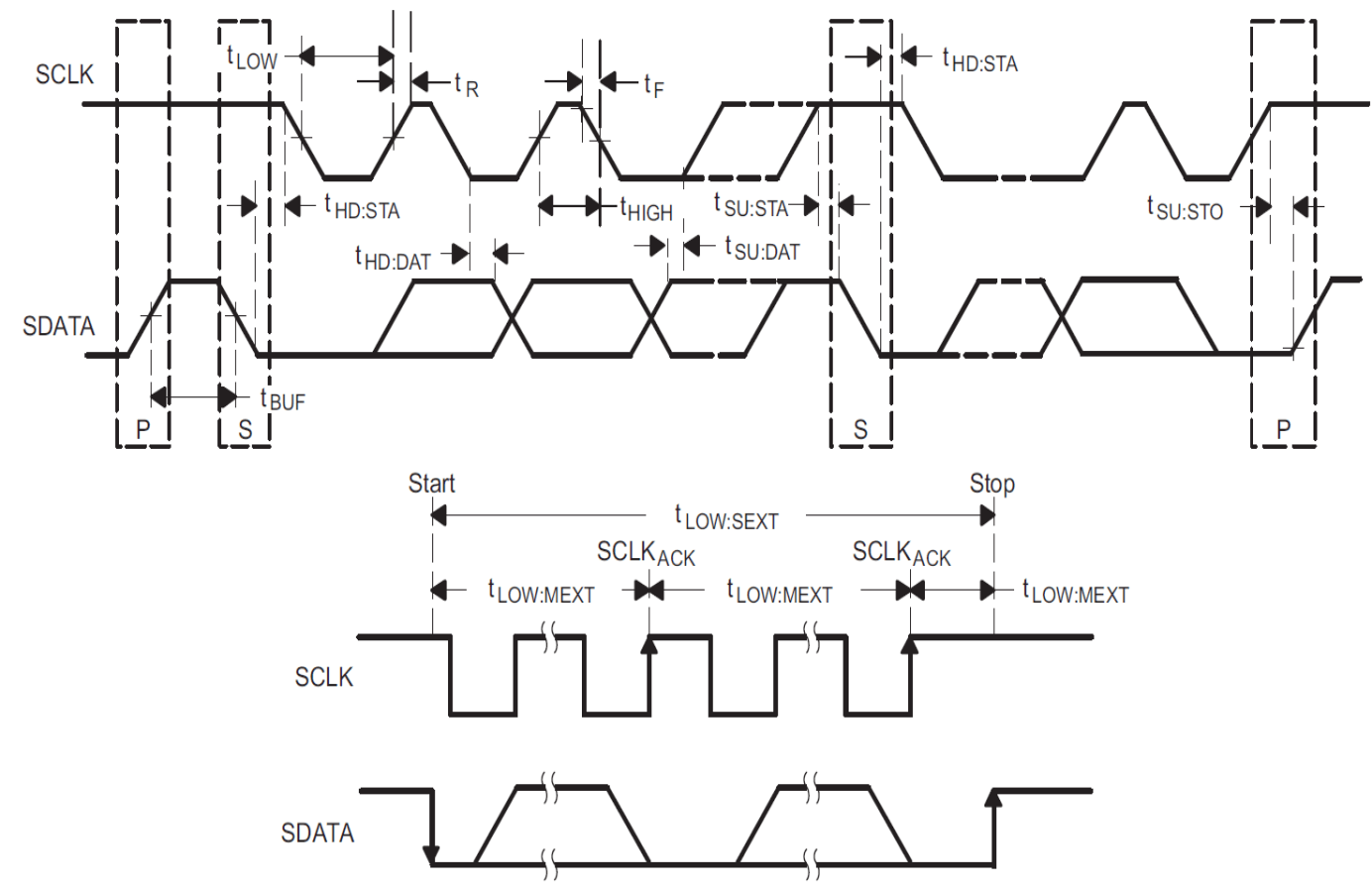
7.12 SMBus Timing Specifications
VCC = 2.4 V to 2.6 V, TA = –40°C to 85°C (unless otherwise noted)| PARAMETER | TEST CONDITIONS | MIN | NOM | MAX | UNIT | |
|---|---|---|---|---|---|---|
| fSMB | SMBus operating frequency | SLAVE mode, SMBC 50% duty cycle | 10 | 100 | kHz | |
| fMAS | SMBus master clock frequency | MASTER mode, no clock low slave extend | 51.2 | kHz | ||
| tBUF | Bus free time between start and stop | 4.7 | µs | |||
| tHD:STA | Hold time after (repeated) start | 4 | µs | |||
| tSU:STA | Repeated start setup time | 4.7 | µs | |||
| tSU:STO | Stop setup time | 4 | µs | |||
| tHD:DAT | Data hold time | RECEIVE mode | 0 | ns | ||
| TRANSMIT mode | 300 | |||||
| tSU:DAT | Data setup time | 250 | ||||
| tTIMEOUT | Error signal/detect | See note(1) | 25 | 35 | ms | |
| tLOW | Clock low period | 4.7 | µs | |||
| tHIGH | Clock high period | See note(2) | 4 | 50 | ||
| tLOW:SEXT | Cumulative clock low slave extend time | See note(3) | 25 | ms | ||
| tLOW:MEXT | Cumulative clock low master extend time | See note(4) | 10 | |||
| tF | Clock/data fall time | (VILMAX – 0.15 V) to (VIHMIN + 0.15 V) | 300 | ns | ||
| tR | Clock/data rise time | 0.9 VCC to (VILMAX – 0.15 V) | 1000 | |||
(1) The BQ78350-R1A device times out when any clock low exceeds tTIMEOUT.
(2) tHIGH:MAX is minimum bus idle time. SMBC = 1 for t > 50 μs causes a reset of any transaction in progress involving the BQ78350-R1A device.
(3) tLOW:SEXT is the cumulative time a slave device is allowed to extend the clock cycles in one message from initial start to stop.
(4) tLOW:MEXT is the cumulative time a master device is allowed to extend the clock cycles in one message from initial start to stop.
 Figure 1. SMBus Timing Diagram