ZHCSED8 November   2015

PRODUCTION DATA.  

  1. 特性
  2. 应用
  3. 说明
  4. 修订历史记录
  5. Pin Configuration and Functions
  6. Specifications
    1. 6.1 Absolute Maximum Ratings
    2. 6.2 ESD Ratings
    3. 6.3 Recommended Operating Conditions
    4. 6.4 Thermal Information
    5. 6.5 Electrical Characteristics
    6. 6.6 Timing Requirements
    7. 6.7 Typical Characteristics
  7. Detailed Description
    1. 7.1 Overview
    2. 7.2 Functional Block Diagram
    3. 7.3 Feature Description
      1. 7.3.1 Charge Pump Control
      2. 7.3.2 Pin Enable Controls
        1. 7.3.2.1 External Control of CHG and DSG Output Drivers
        2. 7.3.2.2 External Control of PCHG Output Driver
        3. 7.3.2.3 Pack Monitor Enable
    4. 7.4 Device Functional Modes
  8. Application and Implementation
    1. 8.1 Application Information
      1. 8.1.1 Recommended System Implementation
        1. 8.1.1.1 The bq76200 is a Slave Device
        2. 8.1.1.2 Flexible Control via AFE or via MCU
        3. 8.1.1.3 Scalable VDDCP Capacitor to Support Multiple FETs in Parallel
        4. 8.1.1.4 Pre-Charge and Pre-Discharge Support
        5. 8.1.1.5 Optional External Gate Resistor
        6. 8.1.1.6 Separate Charge and Discharge paths
    2. 8.2 Typical Applications
      1. 8.2.1 Design Requirements
      2. 8.2.2 Detailed Design Procedure
      3. 8.2.3 Application Curves
  9. Power Supply Recommendations
  10. 10Layout
    1. 10.1 Layout Guidelines
    2. 10.2 Layout Example
  11. 11器件和文档支持
    1. 11.1 文档支持
      1. 11.1.1 相关文档 
    2. 11.2 社区资源
    3. 11.3 商标
    4. 11.4 静电放电警告
    5. 11.5 Glossary
  12. 12机械、封装和可订购信息

封装选项

机械数据 (封装 | 引脚)
散热焊盘机械数据 (封装 | 引脚)
订购信息

10 Layout

10.1 Layout Guidelines

For the following procedure, see Figure 15 and Figure 16.

  1. Place CVDDCP capacitor close to the device.
  2. Place BAT and PACK RC filters close to the device.
  3. Generally, a typical system using an AFE, MCU, and bq76200 usually have a high-current ground trace/plane and low-current ground plane in the PCB layout. If so, the bq76200 ground should be connected to the low-current ground plane of the PCB layout to remove noise affecting the ENABLE signals.

10.2 Layout Example
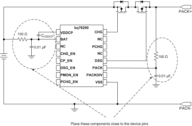
bq76200 Layout.gif Figure 15. Place CVDDCP and Filter Components Close to Device
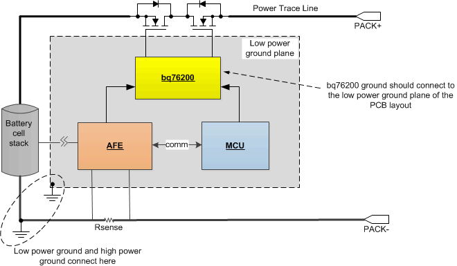
bq76200 Layout_low_power_gndplane.gif Figure 16. Connect bq76200 to Low Power Ground Plane on PCB Layout