ZHCSCI8 May 2014
PRODUCTION DATA.
- 1 特性
- 2 应用范围
- 3 说明
- 4 简化电路原理图
- 5 修订历史记录
- 6 Pin Configuration and Functions
- 7 Specifications
-
8 Detailed Description
- 8.1 Overview
- 8.2 Functional Block Diagram
- 8.3 Feature Description
- 8.4 Device Functional Modes
- 8.5 Register Maps
-
9 Applications and Implementation
- 9.1 Application Information
- 9.2
Typical Applications
- 9.2.1
WPC Power Supply 5-V Output With 1-A Maximum Current and I2C
- 9.2.1.1 Design Requirements
- 9.2.1.2
Detailed Design Procedure
- 9.2.1.2.1 Output Voltage Set Point
- 9.2.1.2.2 Output and Rectifier Capacitors
- 9.2.1.2.3 Maximum Output Current Set Point
- 9.2.1.2.4 TERM Pin
- 9.2.1.2.5 I2C
- 9.2.1.2.6 Communication Current Limit
- 9.2.1.2.7 Receiver Coil
- 9.2.1.2.8 Series and Parallel Resonant Capacitors
- 9.2.1.2.9 Communication, Boot, and Clamp Capacitors
- 9.2.1.3 Application Performance Plots
- 9.2.2 bq5102x Standalone in System Board or Back Cover
- 9.2.1
WPC Power Supply 5-V Output With 1-A Maximum Current and I2C
- 10Power Supply Recommendations
- 11Layout
- 12器件和文档支持
- 13机械封装和可订购信息
6 Pin Configuration and Functions
YFP (42 PINS)
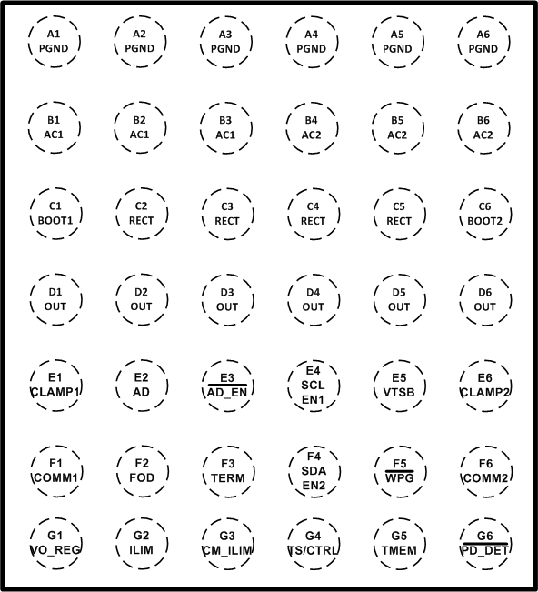
Pin Functions
| PIN | TYPE | DESCRIPTION | |
|---|---|---|---|
| NAME | NUMBER | ||
| AC1 | B1, B2, B3 | I | AC input power from receiver resonant tank |
| AC2 | B4, B5, B6 | I | |
| AD | E2 | I | Adapter sense pin |
| AD-EN | E3 | O | Push-pull driver for dual PFET circuit that can pass AD input to the OUT pin; used for adapter mux control |
| BOOT1 | C1 | O | Bootstrap capacitors for driving the high-side FETs of the synchronous rectifier |
| BOOT2 | C6 | O | |
| CLAMP1 | E1 | O | Open-drain FETs used to clamp the secondary voltage by providing low impedance across secondary |
| CLAMP2 | E6 | O | |
| COMM1 | F1 | O | Open-drain FETs used to communicate with primary by varying reflected impedance |
| COMM2 | F6 | O | |
| CM_ILIM | G3 | I | Enables or disables communication current limit; can be pulled high to disable or pull low enable communication current limit |
| EN1 | E4 | I | EN1 and EN2 are used for I2C communication in bq5020. Ground if not needed. SCL and SDA are used in bq51021. |
| EN2 | F4 | I | |
| FOD | F2 | I | Input that is used for scaling the received power message |
| ILIM | G2 | I/O | Output current or overcurrent level programming pin |
| OUT | D1, D2, D3, D4, D5, D6 | O | Output pin, used to deliver power to the load |
| PD_DET | G6 | O | Open drain output that allows user to sense when receiver is on transmitter surface |
| PGND | A1, A2, A3, A4, A5, A6 | – | Power and logic ground |
| RECT | C2, C3, C4, C5 | O | Filter capacitor for the internal synchronous rectifier |
| SCL | E4 | I | SCL and SDA are used for I2C communication in bq5021. Ground if not needed. EN1 and EN2 are used in bq51020. |
| SDA | F4 | I | |
| TERM | F3 | I | Unused. Float in all WPC receivers |
| TMEM | G5 | O | TMEM allows capacitor to be connected to GND so energy from transmitter ping can be stored to retain memory of state |
| TS/CTRL | G4 | I | Temperature sense. Can be pulled high to send end power transfer (EPT – charge complete) to TX. Can be pulled low to send EPT – Overtemperature |
| VO_REG | G1 | I | Sets the regulation voltage for output. Default value is 0.5 V |
| VTSB | E5 | I | Voltage bias for temperature sense |
| WPG | F5 | O | Open-drain output that allows user to sense when power is transferred to load |