ZHCSEI1 January 2016
PRODUCTION DATA.
7 Detailed Description
7.1 Overview
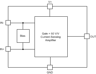
The bq500100 is specially-designed to facilitate foreign object detection (FOD) in wireless charging applications by monitoring the coil supply current. The current-sensing amplifier is able to accurately measure voltages developed across a current-sensing resistor on common-mode voltages that far exceed the supply voltage powering the device. Current can be measured on input voltage rails as high as 20 V when the device is powered off a lower supply voltage.
Low drift characteristics enables high-precision measurements with maximum input offset voltages as low as 200 µV with a maximum temperature contribution of 0.5 µV/°C over the full temperature range of –40°C to +105°C.
7.2 Functional Block Diagram

7.3 Feature Description
7.3.1 High Input Common-Mode Range
The bq500100 can support input common-mode voltages up to 20 V. Because of the internal topology, the common-mode range is not restricted by the supply voltage as long as the input supply stays within the operational range of 2.7 V to 6 V. The ability to operate with supply voltages lower than the input voltage common-mode signal makes the device well-suited for monitoring the current in wireless charging applications where the common-mode voltage varies to obtain a desired amount of power transfer.
When the dc common-mode voltage varies, the effect on the output voltage is very small as a result of the high common-mode rejection. The dc common-mode rejection for the bq500100 is expressed in decibels and is typically as high as 120 dB. In wireless charging applications, the current-sensed rail commonly varies in voltage to adjust for the amount of power transferred by the coil.
7.3.2 High Current-Sense Accuracy Over a Wide Dynamic Range
The offset voltage, gain error, and shunt resistor are the three primary contributors that determine the current measurement accuracy over a specified current range. The offset voltage dominates the error when operating at low current values and the gain error dominates when operating at high current values. The low offset voltage allows use of smaller shunt resistors values. Both the low offset and gain error allow the bq500100 to accurately measure current over a wide dynamic range and still maintain a high level of accuracy.
7.4 Device Functional Modes
7.4.1 Normal Operation
The bq500100 is in normal operation when the following conditions are met:
- V+ is between 2.7 V and 6.0 V
- The common-mode input voltage is less than 20 V
- The differential input signal times gain is less than the supply voltage minus the output voltage swing to V+
- The differential input signal times gain is greater than the swing to GND
- Current flows into the shunt resistor from IN+ to IN– connection points (unidirectional)
When in the normal operating region, the device operates as expected and produces an output voltage that is the gained-up representation of the difference voltage from IN+ to IN–.
7.4.1.1 Device Power-Up
The topology of the bq500100 allows voltages to be present on the inputs before power is applied; therefore, there is no sequencing requirement in regards to the input voltages and the power supply rail for V+. There is a small delay of approximately 50 μs from when power is applied to when the output voltage of the bq500100 settles to the correct voltage level.
7.4.1.2 Input Differential Overload
If the differential input voltage (VIN+ – VIN–) multiplied by gain exceeds the voltage swing specification, the device drives the output as close as possible to the positive supply and does not provide accurate measurement of the differential input voltage. If this behavior occurs during normal circuit operation, then reduce the value of the shunt resistor to avoid this mode of operation. If a differential overload occurs in a fault event, then the output of the bq500100 returns to the expected value approximately 250 μs after the fault condition is removed.